haxxiy said:
Everyone and their mother in the industry knows there are at best a handful of full nodes left and then they are moving on to vertical circuit stacking. This isn't exactly a secret or an opinion: Regardless of TSMC's shenanigans, ITRS's nomenclature has never referred to the physical size of transistors. Historically it was half of the gate pitch which was a close approximation for the smallest feature size of a MOSFET. That hasn't been the case for a long time, however, as logic scales better than the rest of the circuit:
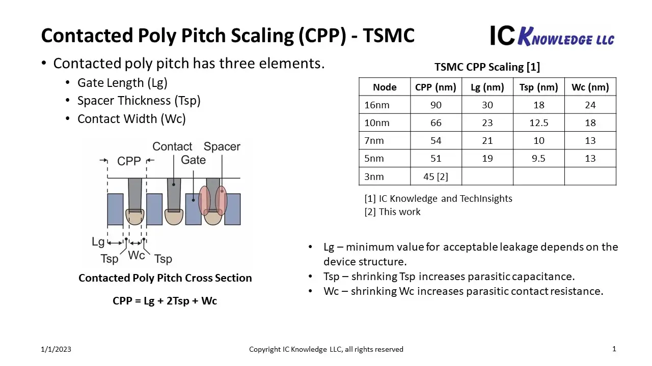
TSMC's 3 nm transistors have logic gates of ~ 15 nm and within them transistors with silicon fins as small as 7 nm wide, which is pretty close to electron mobility collapse from quantum tunneling. Even using theoretical 2D materials and 1 nm transistors as wide as a single molecule isn't going to make matters much better (just ~ 5 times denser than TSMC's N5). Everyone is trying to find smarter solutions for computing problems or trying to find quantum algorithms that actually work (hint: they won't since it's very very very likely that P =/= NP) because they know brute forcing with MOSFETs isn't going to cut the mustard for much longer. |
You should read my post properly as I never stated anything to the contrary.
"Room to exponentially grow" means larger chips, chiplets, stacking and/or shrinks enabled by multi-patterning or new materials. Aka. All of the above.
Research is being done to take things down to potentially (Research is ongoing, but been stupidly promising) 1nm geometrically from the roughly 20nm~ we have today via molybdenum disulfide and single-walled carbon nanotubes, the transistor gate length can potentially be reduced to a size of 1 nanometer, which seems to sidestep a portion of the quantum tunneling issue.
My point is, chip fabrication still has definitely got years of life/improvement left in it, TSMC has plans well into the 2030's.
https://www.tomshardware.com/tech-industry/manufacturing/tsmc-charts-a-course-to-trillion-transistor-chips-eyes-monolithic-chips-with-200-billion-transistors-built-on-1nm-node
But you are right about TSMC's naming, but my point still remains and is factual that it's not actually representative of geometric feature size of a chip.
And chip stacking is a natural progression, once NAND hit a wall in shrinkage's... As NAND becomes less reliable the smaller you go, manufacturers started stacking.

www.youtube.com/@Pemalite


