


By using this site, you agree to our Privacy Policy and our Terms of Use. Close

Forums - Gaming - TECH TALK PT 3: Making a Console. The next next gen.

Happy new year everyone. Its been a while since I added to my tech talk series. On this third part, I will discuss the core considerations that goes into making a console and why.  At the end of this part, I hope you will at least have a better understanding on some of the nitty gritty of console design and when to realistically expect next gen hardware. 

This post will be divided into 2 parts, Powe and Cost 

Disclaimer: The info provided here are mostly my opinion backed on my limited experience in software Dev and general research. So as such this discussion is open to corrections and general input. Enjoy!!!

POWER
Yes. What is inside your console, will determine what it can do. This goes without saying. So let's talk about power. To start things off I will show you a picture of the PS4 APU. Being that its the most powerful of the three current home consoles. so here....
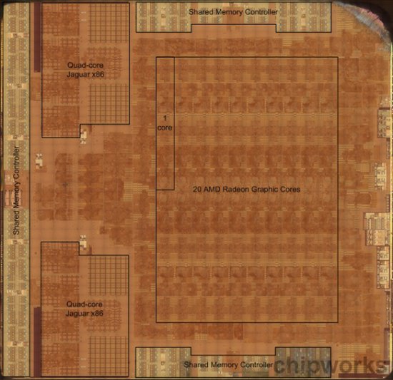
  

So now thats outta the way, let me start by pointing out that everything you see there fits into a ~350mm2 chip (aka die). To put things in perspective, An AMD R9 290 GPU has a footprint of 438mm2. ALL GPU!!!! 

So why does this matter? Well, it just so happens to be that the size of a processor, or more importantly the fabrication process size used in making it is all that really matters when looking at not just how powerful a processor can be but also how much more powerful you can make it. Now both the PS4 and the R9 290 is both made on a 28nm fabrication process. Both processors have a near identical GPU core architecture. Only  major difference is that the PS4 has just 20 of those and the 290 has 40 of them. Granted the PS4 also has 8 CPU cores on its die so it can be forgiven. There are tons of minute other differences like core clocks, memory bus width, ROP number...etc. But those aren't important in this discussion. 

So here is the thing, Loosely speaking, if you can halve the fabrication process size; you can theoretically halve the size of the die or of the cores inside it. In layman terms, PS4 at 14nm fab process can put in twice the number of CPU and GPU cores (which it wouldn't) if the die size remains the same. And at 7nm,  can put in 4 times the number of cores. This is assuming that nothing else changes, this is important cause typically smaller fab sizes doesn't just mean transistor doubling cause chip designers tend to add other components into a die that could benefit their architecture more than just a transistor count bump. 

Note: 14nm will give a 4 times bump and 7nm a 16 times bump. 

What to take from all this, is that to have a  ps5 with 290 card GPU number of cores, the fabrication process has to be small enough to allow them put all those GPU cores and CPU cores on a die not much bigger than 350mm2. Bigger the die, hotter it runs and more power it uses, XB1 has a die size of around 380mm2. That's why its got a bigger fan and bigger chassis to allow for adequate cooling. 

But a jump from 20 GPU cores to 40 is a joke if we are talking PS5 hardware. That's just a 2x bump in core performance. That's not even enough to run games at 4k 60fps. So we need at least a 4/5x bump.  That basically, means we are looking at 14nm fabrication at worst. With 7nm, we get an 8 core CPU with at least 8-12 times the power/ or 4-8 times the transistor count and a GPU with 200-300 cores when compared to what we have in the PS4 today. All in a die size no bigger than 350mm2. Pretty impressive when you think about it. Which brings me to the most important bit.

We are a very very very long way away from a 7nm fabrication process. As it stands, Intel; the leading authority in chip fabrication tech, has just started mass producing 14nm chips. TSCM (the guys that make processors for amd, including the PS4/XB1) are about to start 20nm fabrication and are at best 18 months away from 14nm. Intel expects to start fabricating 7/10nm chips by 2017/2018. Which puts the likes of the people cheap enough to make chips that goes into consoles and GPUs behind by another 18 months.  The next gen doesn't start till we hit 7nm fabrication. 

There is a work around though, which unfortunately could lead to slightly more expensive consoles. Just put the CPU and GPU on seperate chips. 

COST
The two most expensive components in any console are memory and the processor(s). Memory isn't too complicated, you put in what you can afford. So let's again focus on the processor. Recall that long talk we had about chip fabrication? Well it gets worse. Console manufacturers don't get first dibs on a new fabrication process. This means that even if we were to hit 7nm fabrication in 2018, Sony, Microsoft or Nintendo can't order up chips unless they are ready to pay a premium. Which is a no no cause that will mean the consoles in turn get more expensive. So GPU manufactures and apple smartphines get first dibs and everyone else waits until the process matures and yields improve before they can jump in. 

This is unfortunately more straight forward than the first point cause at least that one has a work around. 



Around the Network

PS4 at 14nm fab process can put in twice the number of CPU and GPU cores (which it wouldn't) if the die size remains the same.

It's already 4 times here, 16 times with 7nm. Because of ²


captain carot said:
PS4 at 14nm fab process can put in twice the number of CPU and GPU cores (which it wouldn't) if the die size remains the same.

It's already 4 times here, 16 times with 7nm. Because of ²

Doesnt quite work that way. Halving the fabrication process doesn't give u 4 times the transistor count that's because not everything gets halved exactly in a processor.  You are right if doing just math, but when looking at how processors are made there is more to it than that. 


Yes it does. Normally gates get halved as well. You can as well get the packing density up within one fabrication step. Actually AMD is doing that right now.

RV670's die had 660 Million transistors at 55nm on 192mm². Bonaire has 2.04 billion transistors at 28nm on 160mm². Partially that is due to other structure, Bonaire having cache etc., so a better comparison woild likely be Pitcairn, 4 times the shader units, etc., cache with slightly more die space. 2.8 billion transistors on 212mm².

Now take a look on Carrizo. AMD says Carrizo will be packed much denser so it will have 30% more transistors on the same die space at the same process.

And yes, manufacturing processes are behind, but 20nm is up and running, it's just that at least most of it is reserved for mobile SoC's and Nvidia said they'll likely skip it.
14nm is in early production phase on some fabs. Samsung is at it right now, AMD is right on track according to themselves.


what is the limit?
7nm?
and after this? we wont get more power on a single chip?


Around the Network

I think you're reaching the wrong conclusion here. There is absolutely no need for the next generation to be on 7nm. At least not to be 4 times as powerful. Changes in architecture can have some profound effects on performance.

Best example is Nvidia's Maxwell. The 980 on 398mm² packs more punch than the 780ti on 550mm². Both are produced on 28nm.
In case of an APU we also have to consider that the room for the GPU will get disproportionally bigger than the room for CPU on the die. So 2x the size for both will mean more than 2x the room for the GPU.
Next thing is the form factor of the console itself. With more advanced cooling solutions and maybe a bigger sized console they will be able to sustain a higher clock and pushing the performance even more.

 4x the power on 14nm compared to 28nm is absolutely feasible given appropriate advances in architecture and design of the console.


If you demand respect or gratitude for your volunteer work, you're doing volunteering wrong.

captain carot said:
Yes it does. Normally gates get halved as well. You can as well get the packing density up within one fabrication step. Actually AMD is doing that right now.

RV670's die had 660 Million transistors at 55nm on 192mm². Bonaire has 2.04 billion transistors at 28nm on 160mm². Partially that is due to other structure, Bonaire having cache etc., so a better comparison woild likely be Pitcairn, 4 times the shader units, etc., cache with slightly more die space. 2.8 billion transistors on 212mm².

Now take a look on Carrizo. AMD says Carrizo will be packed much denser so it will have 30% more transistors on the same die space at the same process.

And yes, manufacturing processes are behind, but 20nm is up and running, it's just that at least most of it is reserved for mobile SoC's and Nvidia said they'll likely skip it.
14nm is in early production phase on some fabs. Samsung is at it right now, AMD is right on track according to themselves.

Noted, and you're completely right. will edit my main post. Thanks, must have got my math all mixed up. 


jonathanalis said:
what is the limit?
7nm?
and after this? we wont get more power on a single chip?


For the size of a transistor we are coming closer and closer to physical limits, yes. But there are realistic approaches in other directions.


Right now there is stacked memory like HBM that is supposed to be on AMD'S next graphics cards. Bandwith will get much, much higher this way.

A single gigabyte can right now have 128GB/s this way. Imagine 8GB from the PS4 and you have 1024GB/s. RAM like that is offered by Hynix right now.


And stacked chips could be part of the future of CPU's and GPU's as well.


And there are lots of other attempts, like spintronics. That is a little tough for me to explain correctly in english. But you need much less energy to spin an electron than in traditional electronics. That way you possibly could work with far higher clockspeeds.

Stacked chipdesigns are stuff that already exists and could be used for next gen consoles. As well as present and future manufacturing processes, 11nm or 10nm are a realistic possibility.

There is a ton of stuff that could happen in the next years.


Technical improvements in microelectronics have been losing momentum. Thats true. But at the same time, we have gone down from actual high end hardware in 2005 (Xbox 360) to (lower) midrange in 2013. It's not that unlikely that midrange hardware in 2019 will be an equal step like the last one.


Edit:

@Intrinsic:

No problem. It's not like i dont make mistakes myself.


jonathanalis said:
what is the limit?
7nm?
and after this? we wont get more power on a single chip?


Its getting extremely hard to keep shrinking fab processes. Designers have to become a lot more creative with their chip designs.

But if you want to look at the potential future, you have to accept that there is only so much we can do with silicon based chips. There are experimental alternatives that could completely turn the chip race on its head, but we are at least 20 or so years away from those. 


vivster said:

I think you're reaching the wrong conclusion here. There is absolutely no need for the next generation to be on 7nm. At least not to be 4 times as powerful. Changes in architecture can have some profound effects on performance.


Probably not, but if the time frame for Intel is correct, even with AMD trailling behind for 18 months and supposing that AMD still gets to make the consoles, we get in a decent approximate timeframe of 2019/20, reasonable for 9th gen.

And I would add that aren't just changes in the architecture. If they decide to use a regular CPU + GPU combination instead of APU they will end up with a larger combined die size. However, looking at the lack of overheating issues, pricing and good performance granted by these APUs, I can see them sticking with these design.