fatslob-:O said:
1. Yes the cpu does access the whole DDR3 at 30GB/s max and I believe that 68GB/s was meant for the GPU to the DDR3.
2. Ehh I wouldn`t worry too much about the bandwidth speeds considering that eSRAM is only used too save bandwidth from the GPU having to access the precious 68GB/s.
3. You are right about it missing the DMA on the diagram but I'm willing to bet that it would have to there on the GPU otherwise it wouldn't be able to access the system memory and we all how dumb it would be for the GPU to not have access to the DRAM.
4. You definitely have a point about the move engines not being on this diagram but I don't see it being much of use but I do think that it's used for faster copying of data between the GPU and CPU.
5. I don't think that black line is anything but a mistake plus that interview with the architect of the xbone basically disclosed the eSRAM as nothing more than an evolution of the eDRAM so I think the GPU is the only one with the access to it.
6. I don't think there are any buses between the each of the MMU's considering the diagram doesn't show the MMU's being connected together.
|
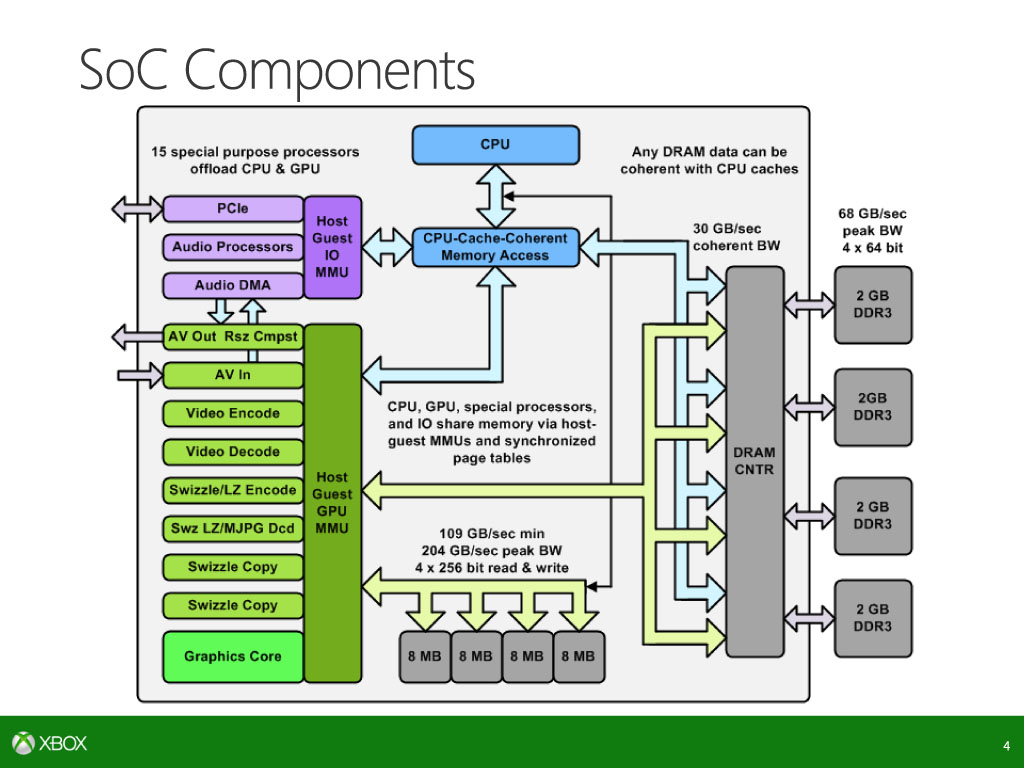
The key part of the diagram is the green rectangle labeled "Host Guest gpu MMU". Lets call it a crossbar switch with tristate buffers and with "stuff" controlling it.
1/2/3. The gpu accesses the ddr3 ram with a maximum of approx 54.6GB/s (unless the memory controllers are "free running" at either 853MHz or 1066MHz). The green rectangle can do alot more (and I mean ALOT more) than what you think. (Note that the ms engineer calls the gpu memory controllers "internal")
4. I meant the four "dme engines". Obviously one of them pushes peripheral data (Kinect, audio, hd). I'd assume at least some of the four dme engines are arbitrated by the "green rectangle"
5. The esram can be accessed by a lot of units via the "green rectangle". The cpu is not one of them (since it is an amd part with apparently ddr3 controller only). Hence the cpu has to do some routing to get to the esram. (Note that the ms engineer calls the cpu memory controllers "external")
6. There is a blue bus between the two mmus
So what is the "green rectangle" labeled Host-Guest gpu mmu? Think of it as a train station where several tracks lead into the station and several tracks lead out of the station. A train incoming on any track can leave the station at any other track. If two trains are incoming, they can do it and leave at the same time if their paths do not cross. Same with data transfers on the XBox.
So what is the difference between "internal" and "external" memory controllers. The four 64bit memory "external" controllers of the cpu are actually (1+3) ddr3 controllers residing near the cpu. This means that controller 1 accesses bytes 0..7 beginning at some address, the other three controllers 2-4 have no free will, they will always access bytes 8..31 (basically there is one master and three slaves, just like in any gpu or cpu). The four 256bit memory "internal" controllers are actually (4+0) sram and ddr3 capable controllers residing near/in the "green rectangle", and, independantly from one another, each of the four controllers can fully address a block of 8MByte of esram (notice there is NO 32MByte block of esram in the XBox One, there are 4 discretely addressable 8MByte blocks of esram). An internal controller can also access the ddr3 ram (assuming at 853MHz). These independant controllers allow that esram can be read and written to at the same time as each controller addresses its own 8MByte block.
What you can also do is the following freak simultaneous memory shuffling:
a) 3 of the internal mcs access the esram at a total of 82GB/s (853MHz). The fourth internal mc accesses the ddr3 at 52.6GB/s (853MHz). A dme copies 15.4GB/s from ddr3 to the fourth esram block. This gives you a maximum data transfer of around 150GB/s.
b) All 4 of the internal mcs access the esram, the cpu accesses the ddr3 at 30GB/s. This gives you 139GB/s data transfer speed.
These are the numbers I see logical. The article writes about 109G/s reads and 109G/s writes to the esram at the same time and gets to 204G/s with dubious "corrections" (even talking about read-modify-write cycles which would be just about the absolute worst thing to do in a multiprocessor environment). Unfortunatly there are only four internal memory controllers, and a memory controller can operate in one direction only at any one given moment (as soon as the address bus is "reserved"). So I wonder how they get there...