By using this site, you agree to our Privacy Policy and our Terms of Use. Close

Forums - Nintendo Discussion - RUMOR: Nintendo Switch 2 leaked factory images/specs/renders

haxxiy said:
 

True, but that would mean Nintendo went for a node that even the PS5 Pro didn't for cost reasons. According to the leaked PCB the die size is around 200 mm², which seems too large for N5/N4 (but also a bit on the too-small side for 8N).

Also, keep in mind that ray-tracing is very CPU and bandwidth-heavy. The advantage will be large for the Series S here, even vs. docked + the best possible clocks for the Switch 2 (not my conclusion, that's from Digital Foundry). The increased memory capacity doesn't mean much if all of it is less than half as fast.

Well the PS5 was on 6nm, a process node that actually saved Sony money when they moved to it from the original PS5 SKU. 4/5 nm actually are slightly cheaper than 8nm because of the higher yields, although probably also slightly more expensive than 6nm. But regardless, I think there is more incentive to go for a more efficient node when building a handheld/console hybrid because you want to get decent performance at low (sub-10) wattages for battery life, and your room for cooling is limited. 

As for the exercise of predicting die-size from the pin layout, I think there is still a bit of uncertainty even there. The twitter poster themselves switched from thinking <8nm, to sure it is 8nm, to indecisive. 

I expect more Switch 2 games to have support for RT than Series S games, although the Switch is going to target much lower effective resolutions and reduced geometry when making comparisons between games with RT on both platforms. 

We've seen memory capacity act as a much larger bottleneck for titles in the last few years than memory bandwidth. When keeping TGP equal, you can do an experiment where you compare how an RTX 3050 (mobile) 6GB (168 GB/s) compares to an RTX 3050ti (mobile) 4GB (192 GB/s) versus an RTX 3050ti 4GB (mobile) and an RTX 2050 mobile (112 GB/s) to see that in more games the RTX 3050 6GB has a bigger performance gap than the 3050ti and the 2050. When capacity becomes a bottleneck, it really becomes a bottleneck whereas you can make some relatively hidden tweaks (to image quality) to make up for the bandwidth bottleneck.

Despite the prior having only 60% of the memory bandwidth of the latter, the RTX 2050 and 3050 (4GB) are within 2% of each-other in terms of performance at 1080p.


Around the Network
siebensus4 said:
160rmf said:

Now that I saw the images... I can conclude that is totally fake. Why people do this btw? Attention? Put pressure on Nintendo? Spare time? Guess we will never know...

The leaker is known to do reverse engineering. This means that the render images were made with the help of the hardware parts he had.

Yeah, I know about that, but the "real" photo still looks like something 3d printed just for fun.

The motherboard could be from some other product and used as base for making this fake joycons and shell. 

Idk, I think if it is already in mass production, we would get something more substantial than that 

Last edited by 160rmf - on 19 September 2024


We reap what we sow

IcaroRibeiro said:
Kyuu said:

Switch's CPU will be a lot weaker than what's inside the Series S though. I think Nintendo's games will target 20-50 GB.

I think 256 GB still small storage even for 20-50GB range. It's barely enough to fill half dozen games... and that's counting only first parties of course. Third parties are likely going above it 

Remember that the Xbox Series S has only 364GB of usable storage space. I don't think that Nintendo's new OS needs that much space, so you probably have ~230GB of usable storage space on the Switch successor, which is not that much less than on the Series S.


siebensus4 said:
IcaroRibeiro said:

I think 256 GB still small storage even for 20-50GB range. It's barely enough to fill half dozen games... and that's counting only first parties of course. Third parties are likely going above it 

Remember that the Xbox Series S has only 364GB of usable storage space. I don't think that Nintendo's new OS needs that much space, so you probably have ~230GB of usable storage space on the Switch successor, which is not that much less than on the Series S.

The solution is to use an SD card. We all have a few spare laying around. 1TB and 1.5TB micro SD cards are cheaper than the Xbox 1TB proprietary cards.


Bite my shiny metal cockpit!

sc94597 said:

Well the PS5 was on 6nm, a process node that actually saved Sony money when they moved to it from the original PS5 SKU. 4/5 nm actually are slightly cheaper than 8nm because of the higher yields, although probably also slightly more expensive than 6nm. But regardless, I think there is more incentive to go for a more efficient node when building a handheld/console hybrid because you want to get decent performance at low (sub-10) wattages for battery life, and your room for cooling is limited. 

TSMC's N6 is just N7 with a slightly tighter pitch, the wafers should cost about the same, so the move made sense in that context.

I haven't seen how much Samsung charges for an 8N wafer, but if it's similar in price to TSMC's 10FF, then N5/N4 is at least two and a half times more expensive and probably much more nowadays (with all the Nvidia bulk orders for Hopper and Blackwell). That makes its cost per area x transistor density about even or worse vs. 8N unless you're gaining on viable chips at the margins of the wafer.

It's still very possible, mind, but at $400 they might be taking a hit depending on the rest of their components. Like, LPDDR5 at 7500 MT/s? NVMe SSDs? Not cheap stuff at all.


Around the Network
Leynos said:
siebensus4 said:

Remember that the Xbox Series S has only 364GB of usable storage space. I don't think that Nintendo's new OS needs that much space, so you probably have ~230GB of usable storage space on the Switch successor, which is not that much less than on the Series S.

The solution is to use an SD card. We all have a few spare laying around. 1TB and 1.5TB micro SD cards are cheaper than the Xbox 1TB proprietary cards.

I think people expecting all next-gen games to run off a slow SD card are in for a wake-up call. There's a reason PS5 and XS restrict next-gen games to SSD's and not USB HDDS. Storage expansion on Switch 2 may be more expensive than you think.

Or we're in for another gen with awful load times on a Nintendo console. The internal storage is 2100mb/s, a 100mb/s SD isn't going to cut it.

Switch 2 will use SD cards, but probably not the ones you've been using everywhere else.

https://news.samsung.com/global/samsungs-new-microsd-cards-bring-high-performance-and-capacity-for-the-new-era-in-mobile-computing-and-on-device-ai

Hopefully the dock also has an nvme slot or at least support for USB SSDs.

Last edited by Zippy6 - on 19 September 2024

haxxiy said:
sc94597 said:

Well the PS5 was on 6nm, a process node that actually saved Sony money when they moved to it from the original PS5 SKU. 4/5 nm actually are slightly cheaper than 8nm because of the higher yields, although probably also slightly more expensive than 6nm. But regardless, I think there is more incentive to go for a more efficient node when building a handheld/console hybrid because you want to get decent performance at low (sub-10) wattages for battery life, and your room for cooling is limited. 

TSMC's N6 is just N7 with a slightly tighter pitch, the wafers should cost about the same, so the move made sense in that context.

I haven't seen how much Samsung charges for an 8N wafer, but if it's similar in price to TSMC's 10FF, then N5/N4 is at least two and a half times more expensive and probably much more nowadays (with all the Nvidia bulk orders for Hopper and Blackwell). That makes its cost per area x transistor density about even or worse vs. 8N unless you're gaining on viable chips at the margins of the wafer.

It's still very possible, mind, but at $400 they might be taking a hit depending on the rest of their components. Like, LPDDR5 at 7500 MT/s? NVMe SSDs? Not cheap stuff at all.

I mean this is pretty outdated at this point, but as of 2022 the cost difference between Sammy 8N and TSMC's 4N was 2.2 times per wafer. That was before Apple moved on to 3N (M2 Max was just about to release) and when Nvidia released Lovelace and AMD released RDNA 3. 

https://www.semianalysis.com/p/ada-lovelace-gpus-shows-how-desperate

"SemiAnalysis sources indicate that the wafer cost of TSMC N5/N4 is more than 2.2x that of Samsung 8nm. With that wafer cost increase comes 2.7x higher transistor density. Nvidia’s top-end die went from 45 million transistors per millimeter squared (MTr/mm2) to 125 MTr/mm2. A fantastic density increase that is closer to 2 process node shrinks than 1 process node shrink. Jensen Huang is right that cost per transistor improvements have slowed significantly."

Going with a newer than 8N process node also allows Nintendo to save on battery and cooling costs. 

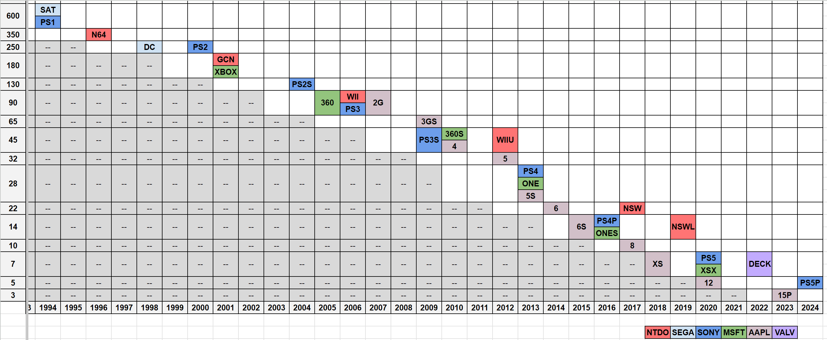
Somebody just posted this chart on Famiboards which shows that Nintendo usually keeps in line what is current when it comes to process nodes. 

Last edited by sc94597 - on 19 September 2024

Zippy6 said:
Leynos said:

The solution is to use an SD card. We all have a few spare laying around. 1TB and 1.5TB micro SD cards are cheaper than the Xbox 1TB proprietary cards.

I think people expecting all next-gen games to run off a slow SD card are in for a wake-up call. There's a reason PS5 and XS restrict next-gen games to SSD's and not USB HDDS. Storage expansion on Switch 2 may be more expensive than you think.

Or we're in for another gen with awful load times on a Nintendo console. The internal storage is 2100mb/s, a 100mb/s SD isn't going to cut it.

Switch 2 will use SD cards, but probably not the ones you've been using everywhere else.

https://news.samsung.com/global/samsungs-new-microsd-cards-bring-high-performance-and-capacity-for-the-new-era-in-mobile-computing-and-on-device-ai

Hopefully the dock also has an nvme slot or at least support for USB SSDs.

I think I will be fine running old Neo Geo games off an SD lol


Bite my shiny metal cockpit!

sc94597 said:

I mean this is pretty outdated at this point, but as of 2022 the cost difference between Sammy 8N and TSMC's 4N was 2.2 times per wafer. That was before Apple moved on to 3N (M2 Max was just about to release) and when Nvidia released Lovelace and AMD released RDNA 3. 

https://www.semianalysis.com/p/ada-lovelace-gpus-shows-how-desperate

"SemiAnalysis sources indicate that the wafer cost of TSMC N5/N4 is more than 2.2x that of Samsung 8nm. With that wafer cost increase comes 2.7x higher transistor density. Nvidia’s top-end die went from 45 million transistors per millimeter squared (MTr/mm2) to 125 MTr/mm2. A fantastic density increase that is closer to 2 process node shrinks than 1 process node shrink. Jensen Huang is right that cost per transistor improvements have slowed significantly."

Going with a newer than 8N process node also allows Nintendo to save on battery and cooling costs. 

Somebody just posted this chart on Famiboards which shows that Nintendo usually keeps in line what is current when it comes to process nodes. 

Good catch---though it seems like TSMC has been hiking prices 5-10% every year since, so the cost gap could still be around 3x come next year if Samsung hasn't changed theirs.

That being said, even the largest Orin would be under 140 mm² on N5/N4, and the T239 should be even smaller, which doesn't seem like a good fit for the PCB.

I'd still guess it's something in between, probably even N6 itself like the other consoles. All the datacenter Amperes were done in TSMC's N7, so there's some precedent for that design from Nvidia too.


haxxiy said:
sc94597 said:

I mean this is pretty outdated at this point, but as of 2022 the cost difference between Sammy 8N and TSMC's 4N was 2.2 times per wafer. That was before Apple moved on to 3N (M2 Max was just about to release) and when Nvidia released Lovelace and AMD released RDNA 3. 

https://www.semianalysis.com/p/ada-lovelace-gpus-shows-how-desperate

"SemiAnalysis sources indicate that the wafer cost of TSMC N5/N4 is more than 2.2x that of Samsung 8nm. With that wafer cost increase comes 2.7x higher transistor density. Nvidia’s top-end die went from 45 million transistors per millimeter squared (MTr/mm2) to 125 MTr/mm2. A fantastic density increase that is closer to 2 process node shrinks than 1 process node shrink. Jensen Huang is right that cost per transistor improvements have slowed significantly."

Going with a newer than 8N process node also allows Nintendo to save on battery and cooling costs. 

Somebody just posted this chart on Famiboards which shows that Nintendo usually keeps in line what is current when it comes to process nodes. 

Good catch---though it seems like TSMC has been hiking prices 5-10% every year since, so the cost gap could still be around 3x come next year if Samsung hasn't changed theirs.

That being said, even the largest Orin would be under 140 mm² on N5/N4, and the T239 should be even smaller, which doesn't seem like a good fit for the PCB.

I'd still guess it's something in between, probably even N6 itself like the other consoles. All the datacenter Amperes were done in TSMC's N7, so there's some precedent for that design from Nvidia too.

Yeah, N7/N6 would at least fit with the historical trend and the fact the professional-level Amperes were on N7 does indeed set the precedent there. Good points.