ethomaz on 18 November 2012
Using Anand's info.
CPU: 32.76mm^2
GPU: 156.21mm^2
3rd die: 2.65mm^2
PS. Too bad Anand sacrificed his Wii to get these info.


Using Anand's info.
CPU: 32.76mm^2
GPU: 156.21mm^2
3rd die: 2.65mm^2
PS. Too bad Anand sacrificed his Wii to get these info.

| ethomaz said: It's ready... good read. http://www.anandtech.com/show/6465/nintendo-wii-u-teardown "There are four 4Gb (512MB) Hynix DDR3-800 devices surrounding the Wii U's MCM (Multi Chip Module). Memory is shared between the CPU and GPU, and if I'm decoding the DRAM part numbers correctly it looks like these are 16-bit devices giving the Wii U a total of 6.4GB/s of peak memory bandwidth. That doesn't sound like a lot, but the Wii U is supposed to have a good amount of eDRAM for both the CPU and GPU to use." Edit - I think Anand made a mistake with the maths... 800Mhz @ 16 bits give it 12.8GB/s and not 6.4GB/s... even so it's too little but explain why the multiplayer in BOPS2 for Wii U have static shadows. |
Not sure he did - 800MHz * 2bytes (16bits) * 4 modules = 6.4GByte/s.
I think you calculated in Gbits: 800MHz * 16bit = 12.8Gbits/s (*4 modules = 51.2Gbits/s = 6.4GBytes/s)
I might be wrong though, not completely sure if this is correct calculus.
|
HoloDust said: Not sure he did - 800MHz * 2bytes (16bits) * 4 modules = 6.4GByte/s. I think you calculated in Gbits: 800MHz * 16bit = 12.8Gbits/s (*4 modules = 51.2Gbits/s = 6.4GBytes/s) I might be wrong though, not completely sure if this is correct calculus. |
I think the right maths is...
800Mhz (the clock) * 2 (bits/line, DDR have 2) * 16bits (bus width) * 4 (modules) = 102,400 Mbits/s = 12,800 MBytes/s = 12.8 GByte/s
Nice... some more info from Anand.
Standby (Power Off) - 0.22W
Wii U Menu (No Disc in Drive) - 31.2W
Wii U Menu (Disc in Drive) - 32.8W
Super Mario U - 33.0W
Netflix Playback - 28.5W
http://www.anandtech.com/show/6465/nintendo-wii-u-teardown
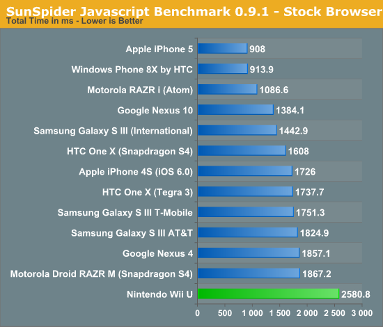
Browser performance...

| ethomaz said:
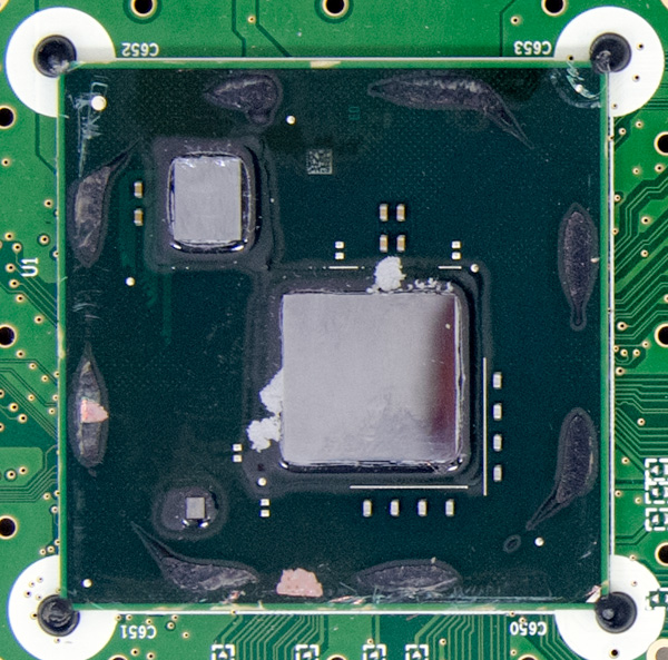
"There are actually three components on this single package, made in at least two different microprocessor fabs. The multicore PowerPC based CPU is the smaller of the two larger chips. This die is made on IBM's 45nm SOI process. The RV7xx derived GPU is the biggest die on the package, and I'm presuming it was made on a 40nm process. I'm assuming the very tiny die in the corner is actually some off-chip memory. Both the CPU and GPU in the Wii U are supposed to have some eDRAM, although the bulk of it is likely dedicated for the GPU. If we assume a 40nm process for the GPU, then we're looking at something a bit larger than the RV740." |
I would assume that is the rumoured ARM core or the DSP rather than some form of cache.

 @TheVoxelman on twitter

ethomaz said:
I think the right maths is... 800Mhz (the clock) * 2 (bits/line, DDR have 2) * 16bits (bus width) * 4 (modules) = 102,400 Mbits/s = 12,800 MBytes/s = 12.8 GByte/s
|
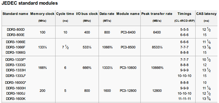
Here is even better math (curiously it's even the correct math since it is directly from Samsung's spec sheet for the chips) :
Data Speed/Pin 2,133 Mbps
Bandwidth/Chip 4.266 GB/s
Burst Length 4, 8
For four chips, this gives you 17Gbytes/s (for 8 cycles = 10ns at 800MHz)
| ethomaz said: Using Anand's info. CPU: 32.76mm^2 GPU: 156.21mm^2 3rd die: 2.65mm^2 PS. Too bad Anand sacrificed his Wii to get these info. |
Why? they did nothing irreversible, screw the thing back together like the PCP guys in their video...
Note that these numbers are complete bullshit. They measured the ceramic chip carrier dimensions, not the die sizes INSIDE the carriers. To know the die sizes (which can be considerable smaller), they would have to actually open the chip carriers. Given there are so many things wrong in that article, I doubt they have someone competent who could actually do that job (and that job would very likely kill the WiiU for good).
|
drkohler said: Here is even better math (curiously it's even the correct math since it is directly from Samsung's spec sheet for the chips) : Data Speed/Pin 2,133 Mbps Bandwidth/Chip 4.266 GB/s Burst Length 4, 8 For four chips, this gives you 17Gbytes/s (for 8 cycles = 10ns at 800MHz) |
Anand "So if I'm reading the Hynix datasheets correctly, that's an 800MHz datarate, which is where the 6.4GBs comes from."
The datasheet is that...
If the memory is 800 datarate (400Mhz) the bandwidth is 6.4GB/s... but I guees he is geting the wrong info... seems like 1600 datarate (800Mhz)... so 12.8GB/s.
Edit - Beyoind3D said it's DDR3-1600 (800Mhz) too http://forum.beyond3d.com/showpost.php?p=1680342&postcount=3263
ethomaz said:
Anand "So if I'm reading the Hynix datasheets correctly, that's an 800MHz datarate, which is where the 6.4GBs comes from." The datasheet is that... |
We are not discussing JEDEC modules made with DDR3 chips, we are talking gDDR3 single chips. Samsung's own data sheets for the very chips win, not some module standard.
|
drkohler said: We are not discussing JEDEC modules, we are talking gDDR3 single chips. Samsung's own data sheets for the very chips win, not some module standard. |
I can read the model number from this picture: http://images.anandtech.com/reviews/video/nintendo/WiiU/DSC_9008.jpg
H5TQ4G63MFR
https://www.skhynix.com/products/computing/view.jsp?info.ramKind=19&info.serialNo=H5TQ4G63MFR
Is that the same model you talking about??? With a 16bits bus interface (64bits for 4 modules) you have 12.8GB/s and not 17.
About Us |
Terms of Use |
Privacy Policy |
Advertise |
Staff |
Contact
Display As Desktop
Display As Mobile
© 2006-2026 VGChartz Ltd. All rights reserved.