HoloDust said:
As for RSX GFLOPS number I took it from wiki, and I find it very strange - actually, to me it makes no sense at all (any one with greater knowledge mind to explain?), so I was guessing it might be in combo with Cell (Cell number is also wrong, full Cell has 230.4, PS3 version can only do 179GFLOPS (1PPE+6SPE, 25.6 per element)), but that doesn't add up good also, so I'm puzzled. Discrepancy in Xenos is more understandable cause of nature of VLIW5 (5th fat one doesn't seem to be used much), so it can be argued that it's 120G Shader ops/s - 240GFLOPS, or 96/192, but I put official specs. |
*** Sorry, my post below is freaken long but I think it'll benefit you from wasting more time beyond worrying too much about theoretical specs ***
Your chart is very pretty but I am gonna drop a bomb on the discussion:
- You cannot under any circumstances compare GLFOPs, Texture, Pixel or Shader performance across different brands of GPUs (especially with different architectures) and even when you are doing it within the same brand (i.e., Nvidia or AMD), sometimes you cannot compare those metrics because AMD and NV upgrade architectures (AMD went from VLIW-5 in R500 in Xbox 360 to VLIW-4 in HD6900 and then to Graphics Core next in HD7000), making the comparison largely meaningless. At best, the comparison can only be made across a specific generation if the underlying architecture is the same (so all GeForce 7s to each other, GeForce GTX400s to each other, all HD7000 series, etc.), but even then you have to be extremely careful. There are various reasons for this:
1) Theoretical #s are meaningless for extrapolating real world gaming performance as they do not account for bottlenecks in a specific SKU. GFLOPs only cover arithmetic calculations performed by the shaders of the GPU and tell us nothing about other bottlenecks on the GPU architecture. To perform anti-aliasing for instance, we need a ton of memory bandwidth. GFLOPs tell us nothing about memory bandwidth. Then you have architecture inefficiencies. RSX is a fixed vertex/pixel shader architecture with fragment pipelines vs. GeForce 8 which is a unified shader architecture. What that means is the latter has shaders that can perform pixel and vertex operations but the former only has 24 pixels and 8 vertex shaders. If a game needs more pixel shaders, RSX is stuck with 24 at max. A unified architecture can seamlessly change this to 30/2, 24/8, 16/16, etc. The former has a lot more inefficiencies but looking at FLOPs won't tell us that. Comparing theoretical GLFOPs, TMUs, Pixel shading power will not tell you what those architectures can actually put down in a game in the real world due to their specific efficiencies (I will provide examples to prove this below). Some games need more texture performance, some need more shaders, some need compute shaders. You can have 10x the texture performance of a competing GPU but if you are compute shader limited for calculating HDAO/super-sampled AA on textures in Far Cry 3, your GPU is bottlenecked.
Let's tackle the FLOPs more closely.
2) GFLOP performance does NOT directly translate into gaming performance. Comparing FLOPS is marketing unless you know for sure what it is you are you are using the GPU for. For example, if you are performing SHA-256 password hashing, the GPUs ALUs (in this case shaders/CUDA cores) perform a 32-bit "right rotate operation". Modern AMD GPUs can do this in a single instruction, but NV's require 3 separate instructions (2 shifts + 1 add). If you only compared GFLOP performance, you do not know how the GPU can run different instructions based on this # alone. Each architecture is different. Complicating matters, games do not only use shaders/ALUs but GFLOPs only looks at shaders/ALUs. First we need to understand what a GFLOP is.
"FLOPS (or flops or flop/s, for floating-point operations per second) is a measure of computer performance, especially in fields of scientific calculations that make heavy use of floating-point calculations, similar to the older, simpler, instructions per second."
The problem is there are various floating point instructions. You can have single precision, double precision floating point operations (for this type there is a 24x penalty on GTX680, 16x penalty on HD7870 and only a 4x penalty on HD7970 but it tells you nothing about games). But just so you can wrap a real world example around this, I'll show you why FLOPS are meaningless:
Floating Point operations - calculated off the shaders/cuda cores/stream processors in the GPU:
GTX580 = 512 CUDA cores x 772mhz GPU clock x 2 for Shader clock (as shaders operate at 2x the speed of the GPU in this architecture) x 2 Instructions per clock (this is 2 floating ops/clock cycle) / (1000 Megaflops in 1 Gflop) = 1581 GFlops or 1.581 Tflops
GTX680 = 1536 CUDA cores x 1058mhz GPU clock (same as shader clock so no need to multiply by 2) x 2 Ops/clock / (1000 Megaflops in 1 Gflop) = 3250 Gflops or 3.25 TFlops
HD7970 Ghz Ed. = 2048 Stream processors/shaders x 1050mhz GPU clock (same as stream processor clock) x 2 Ops/clock / (1000 Megaflops in 1 Gflop) = 4300 Gflops or 4.30 Tflops
Now from the above, you might think that GTX680 is 2.055x faster in games than GTX580 and HD7970 GE is 32% faster than GTX680. We know for a fact this is not true: http://www.techpowerup.com/reviews/HIS/HD_7970_X_Turbo/28.html
3) OK next, moving on to addressing the comparison of things like Textures (TMUs), Pixel shading power and ROPs and so on. All those are again meaningless without knowing how the architecture works.
I'll use AMD this time to show you how anyone can make a major mistake using this type of theoretical comparison.
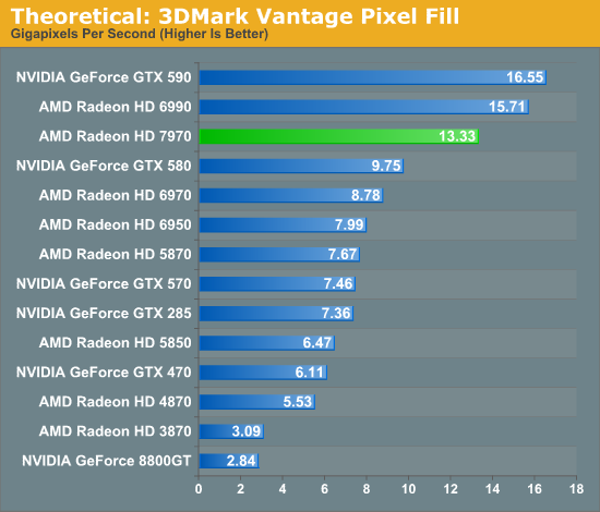
Theoretical Pixel Shading Power:
HD6970 = 32 ROPs x 880mhz GPU clock = 28.16 GPixels/sec
HD7970 = 32 ROPs x 925mhz GPU clock = 29.6 GPixels/sec
It's logical to conclude that HD7970 Ghz Ed. has 5% more Pixel shading performance, correct? Incorrect. The theoretical numbers didn't explain how the architecture changed from HD6000 to HD7000 series. HD7970 uses Graphics Core Next architecture, which unlike VLIW-4 of HD6970, decouples the ROPs from the memory controllers and thus the ROPs are fed more memory bandwidth directly via a crossbar. To make a story short, HD7970 same 32 ROPs are 50% more efficient, or HD6970 can never reach its theoretical rate of 28.16 GPixels because it's ROPs are much more inefficient. When you run a real world test, you see the real Pixel shading throughput that is 52% greater, not 5%.
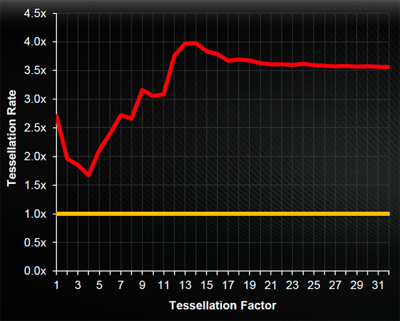
Now you are starting to see slowly how comparing specs is becoming meaningless. More evidence? For example, a key feature of DX11 games is tessellation. Even if you dove deeper into the specs of HD6970 vs. HD7970, you'd find that HD6970 has 1 Geometry engine and HD7970 has 2. These geometry engines are responsible for performing tessellation. If you looked at GPU clocks of HD6970 of 880mhz and HD7970 of 925mhz, you might say OK, I think HD7970 would be slightly more than 2x faster. That seems like a reasonable assumption. It would be incorrect again.
If you just looked at specs like GFLOPs, Textures, Pixels and Memory Bandwidth, you would miss an integral part of next generation games - geometry engine performance. Even if you compared 1 Geometry engine of HD6970 to 2 of HD7970, you'd have to read deeper to understand that in Graphics Core Next of HD7970 (unlike VLIW-4 of HD6970), the parameter cache was enlarged, allowing increased vertex re-use and off-chip buffering. The DX11 geometry/tessellation preformance increased 1.7-4x, not the "slightly more than 2x faster" I noted above.
It gets MORE complicated since modern games now use Pixel shaders, geometry shaders, vertex shaders, textures, z-culling, and a new type of shaders called compute shader. There is a relationship between memory bandwidth and ROPs and how they are connected to anti-aliasing. All of these differ in efficiencies not just across AMD and NVidia but against those brands themselves since you cannot just compare Nvidia's GeForce 7 with GTX600 or HD6000 to HD7000 as both of those are entirely different architectures.
To make things easier, IGNORE ALL THESE THEORETICAL SPECS. Focus on 3 things only:
1) Find out exactly what architecture is used in the GPU of a next gen console, or at least the codename for the chip so we can back into the architecture (G70/71 = RSX, R500 = Xenos of Xbox 360, etc.)
2) Look up the specifications on this website (http://www.gpureview.com/show_cards.php) and compare them to the specs of the GPU in the console. Do they match? If so, proceed to point #3, if not proceed to point #4.
3) Look up the Voodoo GPU Power # in this chart corresponding to the GPU that matches the console's GPU specs (http://alienbabeltech.com/abt/viewtopic.php?p=41174). These #s are actual gaming performance in real world games, compiled into 1 number for simplicity after reviewing hundreds of reviews of PC hardware parts in games. If specs match, it's easy to compare as dividing 1 number by the other to see % difference. That's it, you are done. So for example, HD7850 2GB is 139 VP and X1800XT is 16.7 VP (~ performance of Xbox 360's GPU). That means HD7850 2GB is going to be 8.3x faster in games on average.
4) If specs do not match, the GPU may be a mobile version of a desktop part. You'd need to start looking here (http://www.notebookcheck.net/Mobile-Graphics-Cards-Benchmark-List.844.0.html). More likely than not, the GPU in next generation consoles will be a variant of a Mobile GPU or even a custom GPU/APU. If specs do not match (like RSX in PS3 is a 7950GT with 50% less ROPs and 50% less memory bandwidth), then you are going to have to start doing estimates and reducing performance per chart in #3 and trying to figure out where the architecture and specs fit relative to desktop GPUs in 3). So in the chart in #3, a full-blown HD7950GT is 19.9 VP but we know RSX in PS3 has units cut. We know for sure it's below this mark.
Hope this saves you a lot of headache since comparing theoretical numbers is just going to mislead you guys!!! I know I already posted something like this here but I see it's being ignored. You are going to find yourself spinning wheels trying to compare theoretical #s that have no relation to each other and it's just going to confuse you or lead to incorrect conclusions.
First find out what the underlying architecture is, then focus on the specs, but ONLY so you can look up real world gaming performance in that Voodoo GPU power chart.
What makes things even more complicated is that Xbox 720 might use PowerPC CPU and PS4 might use x86 CPU. Even if we know the GPU comparison, it'll become very difficult to compare the CPUs. Then there is eDRAM which complicates matters as it can be used reduce the performance hit a GPU incurs when accelerating anti-aliasing, somewhat making up for lost memory bandwidth. And there is always a possibility PS4/Xbox 720 could use some truly innovative technologies to reduce latencies like die stacking (http://semiaccurate.com/2012/09/06/die-stacking-has-promise-and-problems/). But let's not even go there :)