Trumpstyle said:
Bofferbrauer2 said:
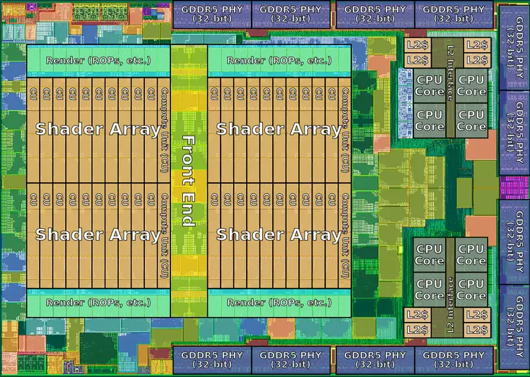
64CU? That would still be about 400m2 in Navi (RX5700 with 40CU comes to ~260mm2), and thus a pretty expensive chip to produce. I doubt it will get such a big chip and rather rely more on GPU clock, as that alone could make the console probably $50-100 more expensive than a chip with less than 300m2.
|
Yep probably even higher, I always assumed Sony/Microsoft will use 7nm EUV because of my estimated die sizes, I ran the numbers for 64CU's:
251mm2 (Navi10) + 54.36mm2 (24CU) + 20mm2 (ray-tracing) + 40mm2 (cpu) + 32.64mm2 (2x 64-bit controllers) + 50mm2 (wasted die area) = 448mm2 on tsmc 7nm.
EUV reduces die area by 20% but I don't think it will have perfect scaling so I used 15% instead.
448mm2 * 0.85 = 380.8mm2 on tsmc 7nm EUV.
Ofc it could be smaller depending on how much wasted die area Microsoft can reduce, Xbox one X had about 50mm2 wasted die area and PS4 pro 70mm2 wasted die area, going from 16nm to 7nm might reduce wasted die area, I don't know.
What's interesting is that his TF number for Xbox series X is almost certainly a Devkit number and not retail version, the verified insider says PS5 has higher TF than Xbox series X but the retail version might be lower, all from 10.1-11.2TF as the memory bandwidth for PS5 just isn't there for 12TF.
|
I don't think they will make one monolithic chip with CPU and GPU in one. More likely they will put CPU and GPU under one hood (heatspreader) but keep them separated chips to save on costs.
Also, how did you get to 40mm2 for the CPU? A Zen 2 chiplet, which is pretty much what would get used in the consoles and the part used in an APU, is 80mm2. 40mm2 would only result into 4c/8t unless you'd remove most of the L2+L3 caches - but that would drastically slow down the chip. You might have confused the size of a chiplet with the one of a CCX, of which there are 2 in a chiplet.
A similar point could be made for the I/O, which is a bit more than just the 64-bit controllers. For reference, the I/O chip in Ryzen, while still produced in a 12nm process, is still 125mm2 and has over two thirds of the amount of transistors of a Zen 2 chiplet. Of course much of that is unnecessary on a console, but not all. Expect more like 40-50mm2 for the entire I/O than just 32mm2.
The wasted area is mostly over-provisioning. In this case for instance, instead of having all 64CU working, they could only have 56-60 of them running (at a higher clock speed to compensate) and have the rest as reserve to allow even not fully functioning chips to be used for the consoles, drastically increasing yield. With 64 working CU that would certainly mean 72 CU in production and a chip die larger than the one of the Vega VII, which was already 336mm2... in 7nm I might add.
As you can see, we would be pushing close to 500mm2 by now, way to large for a single chip in a console. Putting CPU and IO into a different chip would make it much cheaper in production and keep the sizes below 400mm2.