By using this site, you agree to our Privacy Policy and our Terms of Use. Close
Trumpstyle said:
Bofferbrauer2 said:

I don't think they will make one monolithic chip with CPU and GPU in one. More likely they will put CPU and GPU under one hood (heatspreader) but keep them separated chips to save on costs.

Also, how did you get to 40mm2 for the CPU? A Zen 2 chiplet, which is pretty much what would get used in the consoles and the part used in an APU, is 80mm2. 40mm2 would only result into 4c/8t unless you'd remove most of the L2+L3 caches - but that would drastically slow down the chip. You might have confused the size of a chiplet with the one of a CCX, of which there are 2 in a chiplet.

A similar point could be made for the I/O, which is a bit more than just the 64-bit controllers. For reference, the I/O chip in Ryzen, while still produced in a 12nm process, is still 125mm2 and has over two thirds of the amount of transistors of a Zen 2 chiplet. Of course much of that is unnecessary on a console, but not all. Expect more like 40-50mm2 for the entire I/O than just 32mm2.

The wasted area is mostly over-provisioning. In this case for instance, instead of having all 64CU working, they could only have 56-60 of them running (at a higher clock speed to compensate) and have the rest as reserve to allow even not fully functioning chips to be used for the consoles, drastically increasing yield. With 64 working CU that would certainly mean 72 CU in production and a chip die larger than the one of the Vega VII, which was already 336mm2... in 7nm I might add.

As you can see, we would be pushing close to 500mm2 by now, way to large for a single chip in a console. Putting CPU and IO into a different chip would make it much cheaper in production and keep the sizes below 400mm2.

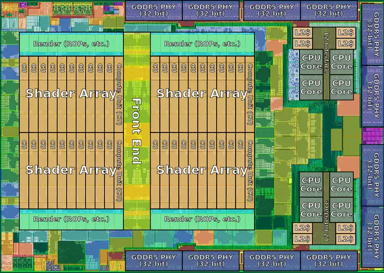
The GPU (Navi10) already has a I/O die, there's no need for another one. As for the CPU, 2x zen2 CCX are 70mm2, you cut off 24mb of the GameCache it should land around 40mm2, and I think the devkit has all 64CU's activated so Microsoft will simply disable 4/8 CU's and up the clock-speed to hit 12TF. There's no 72CU's.

Wasted die area, what I mean by that is you can't pack everything into a perfect Square/rectangle, here's a die shot of Xbox one X:

Even though we can't see the I/O stuff, you can see the CU's, the 32-bit controllers and the 2 CPU clusters aren't packed into a perfect Square/rectangle that's what I mean by wasted die area. You will always have wasted die area.

Edit: Forgot about double chip, Microsoft has already shown a monolith die in there E3 video, it will be a APU/SOC.

Often you have areas of "Dark Silicon" in order to reduce leakage.
You also often have extra functional units in order to increase yields incase part of the chip is non-functional.

Some parts of a chip are also duplicated on other parts of the chip because it works out to be cheaper than actually putting in the routing.

There are lots of considerations that go into chip design.

About 40-50mm without the caches seems very plausible for Zen2 chiplets.


--::{PC Gaming Master Race}::--