Ok, so here's a kind of recap about Pascal and the Tesla P100.
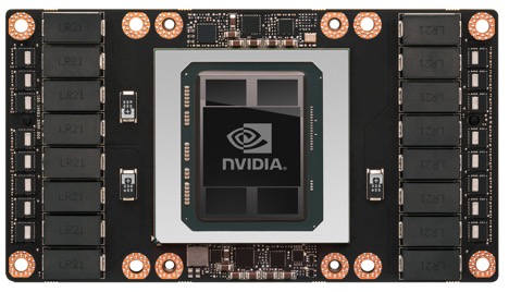
This is Tesla P100:
And this is Pascal's P100 core diagram:
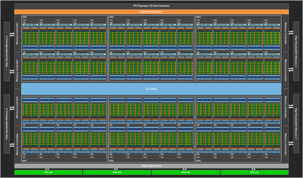
First things first: The chip has 8x512-bit memory controllers for a total of 4096-bit memory bus width. This is because the P100 uses 4xHBM2 memory stacks instead of GDDR5.
The GPU itself is compromised of 6 GPCs (Graphics Processor Cluster), with each cluster comprised of 10 SMs (Streaming Multiprocessor). This is a departure from Maxwell and its 4 SMs for each GPC, of which also had 6 GPUnits.
Now let's take a closer look at a SM unit
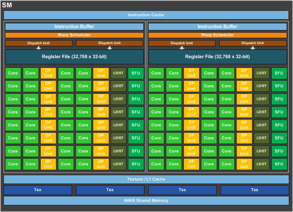
As you can see, each Pascal SM is comprised of 64 CUDA cores (or shaders) and 4 Texture Units, whereas Maxwell also had 4 Texture Units but the Shader Units count was twice as much with 128.
That's because Nvidia has focused a lot on the computing side of things, improving its single precision (FP32) performance but specially it's Double Precision (FP64) results, achieving a whooping 1:2 ratio between single and double precision compared to the paltry 1:32 ratio of Maxwell (that was beated by Kepler).
Finally, the chip features 14MB of shared register files and 4MB of L2 cache.
And here is a table comparing the Tesla P100 with the previous Tesla products and top-end cards:
|
Tesla P100 |
|
Tesla M40 |
GTX Titan X |
|
Tesla K40 |
GTX Titan Black |
| GPU |
GP100 |
|
GM200 |
GM200 |
|
GK110B |
GK110B |
| Architecture |
Pascal |
|
Maxwell 2 |
Maxwell 2 |
|
Kepler |
Kepler
|
| GPC |
6 |
|
6 |
6 |
|
5 |
5 |
| SMs |
56 |
|
24 |
24 |
|
15 |
15 |
| CUDA Cores/SM |
64 |
|
128 |
128 |
|
192 |
192 |
| CUDA Cores |
3584 |
|
3072 |
3072 |
|
2880 |
2880 |
| Texture Units/SM |
4 |
|
4 |
4 |
|
16 |
16 |
| Texture Units |
224 |
|
192 |
192 |
|
240 |
240 |
| ROPs |
- |
|
96 |
96 |
|
48 |
48 |
| Core Clock |
1328 MHz |
|
948 MHz |
1000MHz |
|
745 MHz |
889MHz |
| Boost Clock |
1480 MHz |
|
1114 MHz |
1075MHz |
|
810/875 MHz |
980MHz |
| Memory Type |
HBM2 |
|
GDDR5 |
GDDR5 |
|
GDDR5 |
GDDR5 |
| Memory Clock |
1,4GHz |
|
6GHz |
7GHz |
|
6GHz |
7GHz |
| Memory Bus Width |
4096-bit |
|
384-bit |
384-bit |
|
384-bit |
384-bit |
| Memory Bandwidth |
720GB/sec |
|
288GB/sec |
336GB/sec |
|
288GB/sec |
336GB/sec |
| VRAM |
16 GB |
|
12 GB |
12GB |
|
6 GB |
6GB |
| TDP |
300 Watts |
|
250 Watts |
250W |
|
235 Watts |
250W |
| Transistor Count |
15.3 Billions |
|
8 Billions |
8 Billions |
|
7.1 Billions |
7.1 Billions |
| Single Precision FP32 |
10.6 TFLOPS |
|
6.8 TFLOPS |
6.14 TFLOPS |
|
4.29 TFLOPS |
5.1 TFlops |
| FP64 |
1/2 FP32 |
|
1/32 FP32 |
1/32 FP32 |
|
1/3 FP32 |
1/3 FP32 |
| Double Precision FP64 |
5.3 TFLOPS |
|
213 GFLOPS |
- |
|
1.43 TFLOPS |
- |
| Manufacturing Process |
TSMC 16nm |
|
TSMC 28nm |
TSMC 28nm |
|
TSMC 28nm |
TSMC 28nm |
| GPU Die Size |
610 mm² |
|
601 mm² |
601 mm² |
|
551 mm² |
551 mm² |
Of course, anyone expecting the upcoming GTX 1080/1070 (or whatever they are called) to be as big as P100 will be disappointed. Expect the 1080/1070 to be based on a GP 104 chip with the number of Graphics Processor Clusters reduced to 4, and the 1060/1050 to have 2 GPCs.
Please excuse my bad English.
Currently gaming on a PC with an i5-4670k@stock (for now), 16Gb RAM 1600 MHz and a GTX 1070
Steam / Live / NNID : jonxiquet Add me if you want, but I'm a single player gamer.


 .
.

 Essay Pro