By using this site, you agree to our Privacy Policy and our Terms of Use. Close

Forums - Nintendo Discussion - Wii U GPU Die Image! Chipworks is AWESOME!

AnthonyW86 said:
Well i guess 1.5 times the processing power and twice the video memory is pretty good, though it isn't enough for multi-platform games at 1080P. Just hope the CPU is better than it looks.

Man that display pic. Yuck. I am sure though it can run Crysis. Should be fine. 


Around the Network
Soundwave said:

Nintendo is over engineering and over thinking their hardware.

They should've just used an AMD E6760, it would've saved them a lot in R&D costs and given them higher performance for probably an equivalent cost (maybe even cheaper) since it wouldn't be such a custom part (500+ GLFOPS easy). Third parties would like it better because it'd be easier to move PC games to the platform, and lets face it, Nintendo's own teams do fine on any hardware. And an E6760 only draws 35 watts and that's with GDDR5 memory, axe that and it would be even lower.

You could customize it a bit I'm sure too.

Insisting on such proprietary, customized hardware is killing Nintendo on cost, and they're not even getting great performance bang for their buck. For $350+  IMO, even with a 6 inch low-res LCD screen on the controller, they could've gotten a better piece of hardware from AMD.

I think this is where Yamauchi and Iwata are different, Yamauchi would opt to go with more standardized components if it meant cheaper cost/better performance.


This is what I was just thinking. The console is not really powerful, Bluray is much more common nowadays than in 2006 (and without royalties since it doesn't plays movies) and the screen on the controller is not that hi-tech... AND STILL Nintendo manages to lose money with every Wii U sold! I really don't understand what happened here. Maybe the GPU is so customized that it's expensive to produce en masse, or the (bad) engineering done at ( or "for") Nintendo was really expensive, or some supplier got Nintendo into a really bad business. Maybe Nintendo should start to engineer their future consoles in America or something, and leave only the concept to the Japanese.

About the bolded part... I'm not sure that Yamauchi was so different...  See the Nintendo 64 for example.


TheLastStarFighter said:
Clearly the flopzone in the upper right of the pasty brown map diagram shows a meta-multiplier for the quark generator in the first quandrant. The unique architecture in the layout allows for cyclic interchange increasing processing output by about 347%. The end result is a chip which could potentially out-perform a PS3 by about 6.14X, which is quite remarkable, though the nano inhibitor in the bottom right will probably form a bottleneck in real-world application, making true output about 3.9X PS3 levels.


Hahah! :D


The BuShA owns all!

green_sky said:
I scrolled entire thread looking for BlueFalcon post. He hasn't posted yet. Some one make sense out of this.

I'll try my best. Here is my initial wild stab.

Starting with RV770 (HD4870) as that's the complete R700 GPU. 

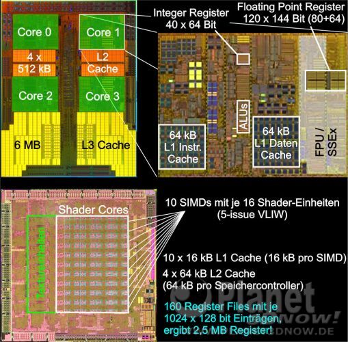
Green Square is your Texture Block Unit. If you count down vertically, you get 10 of those. Each Green square has 4 TMUs. So the total # of TMUs in RV770 is 10 Texture Block Units x 4 TMus per block = 40 TMUs

On the right hand side, you have Blue Rectangle I highlighted. Those are SIMDs (or shader cores). In RV770, it looks like there are 4 complete squares inside 1 Blue Rectangle. If you count down vertically again, the total # of SIMD blocks is 10. Each SIMD block array is made up of 16 VLIW-5 shader units, giving us a total of 16x5 = 80 Shaders per 1 SIMD block, for a total of 80 Shaders per SIMD x 10 SIMDs = 800 Shaders in RV770.

Notice that since 1 full length SIMD block has 4 distinct sections, we end up with 80 Shaders / 4 = 20 Shaders per each sub-block in 1 SIMD array.

Here are the building blocks for RV770 in simpler terms:

You can see that there are 10 SIMDs with 16 VLIW-5 shaders:
OK now the Wii U:

Now notice how each SIMD array has 3 full blocks but 2 "half-blocks" above and below the 3 full ones? If those are somehow active, you end up with 3+ 1/2+1/2 = 4 Sub-blocks per 1 SIMD or a total of 4x 20 = 80 Shaders per SIMD. 8 Total SIMDs x 80 Shaders would give 640 Shaders (exactly the same as RV740).

The missing piece are ROPs. We know the Wii U has 64-bit memory interface because it has 4x 256MB chips over 16-bit bus each. Therefore, the GPU has half the memory blocks of RV740. RV740 had 32 TMUs and 16 ROPs, with 128-bit bus. This matches up perfectly with HALF of RV740's 16 TMUs / 8 ROP / 64-bit bus.

http://www.gpureview.com/show_cards.php?card1=564&card2=612

At 40nm, the RV740 crams 826 million transistors into a 137 mm² die. (http://techreport.com/review/16820/amd-radeon-hd-4770-graphics-processor)

This could explain why Nintendo sacrificed half the TMUs and ROPs or RV740 (and coincidentally explains the 64-bit halving of memory bandwidth from RV740's full 128-bit). 

I can't but help thinking since Nintendo is striving to maximize every mm2 here, I am going with a prediction that the 2 "half-blocks" in the SIMD arrays are enabled. So probably the 8 SIMD x 80 Shaders per block = 640 SPs in total, exactly like in RV740, is retained.

http://techreport.com/review/16820/amd-radeon-hd-4770-graphics-processor

My pure guess estimates:

RV740 derived 40nm GPU @ 550mhz

480 - 640 SPs 

16 TMUs (Half of RV740)

8 ROPs (Half of RV740s = 2 Render Back Ends instead of 4 on RV740)

64-bit x 1 memory bandwidth


@BlueFalcon

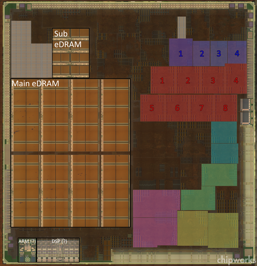
What you listed in BLUE and GREEN are eDRAM... the GPU part is on the right side.


Around the Network
BlueFalcon said:
green_sky said:
I scrolled entire thread looking for BlueFalcon post. He hasn't posted yet. Some one make sense out of this.

I'll try my best. Here is my initial wild stab.

Starting with RV770 (HD4870) as that's the complete R700 GPU. 

Green Square is your Texture Block Unit. If you count down vertically, you get 10 of those. Each Green square has 4 TMUs. So the total # of TMUs in RV770 is 10 Texture Block Units x 4 TMus per block = 40 TMUs

On the right hand side, you have Blue Rectangle I highlighted. Those are SIMDs (or shader cores). In RV770, it looks like there are 4 complete squares inside 1 Blue Rectangle. If you count down vertically again, the total # of SIMD blocks is 10. Each SIMD block array is made up of 16 VLIW-5 shader units, giving us a total of 16x5 = 80 Shaders per 1 SIMD block, for a total of 80 Shaders per SIMD x 10 SIMDs = 800 Shaders in RV770.

Notice that since 1 full length SIMD block has 4 distinct sections, we end up with 80 Shaders / 4 = 20 Shaders per each sub-block in 1 SIMD array.

Here are the building blocks for RV770 in simpler terms:

OK now the Wii U:


I'm pretty sure the part you marked as the 8 SIMD blocks is the eDRAM.


Other IO interfaces in the chip...


ethomaz said:

@BlueFalcon

What you listed in BLUE and GREEN are eDRAM... the GPU part is on the right side.

ghost_of_fazz said:

I'm pretty sure the part you marked as the 8 SIMD blocks is the eDRAM.

Ya, I was struggling with that. I couldn't reconcile what the other half of the GPU was. I just looked at RV770 diagram and tried to extrapolate how the building blocks might look like. It was a pure guess on my part. However, now if the 2 types of eDRAM take up nearly 40% of the die from that picture and the entire GPU die is just 150mm2, that GPU is going to be extremely underpowered even compared to RV740. If RV740 fits 640 SPs, 32 TMUs, 16 ROPs, and nearly half of the die is taken up by eDRAM, then I doubt they can fit more than a 320 SP, 16 TMUs, 8 ROP 40nm GPU on the right hand side of the die. That would be an even weaker GPU than I estimated. I suppose the 35W load power consumption in games is a giveaway that this console is very underpowered. 

Considering the Wii U sells for $300-350, it's shocking how they butchered the GPU and CPU components so much. I mean even if it's a full 320 SPs/ 16 TMU / 8 ROP part, the 12.8GB/sec memory bandwidth is crippling. This seems like wasting millions of dollars on a custom part that would have been outperformed by an off-the-shelf 40nm RV740 GPU with 0 customization! I have no idea what Nintendo was thinking on this one. I am thinking the GPU is barely 50% faster than the 48 SP VLIW-5 R500 in Xbox 360, if that. 


BlueFalcon said:
Ya, I was struggling with that. I couldn't reconcile what the other half of the GPU was. I just looked at RV770 diagram and tried to extrapolate how the building blocks might look like. It was a pure guess on my part. However, now if the 2 types of eDRAM take up nearly 40% of the die from that picture and the entire GPU die is just 150mm2, that GPU is going to be extremely underpowered even compared to RV740. If RV740 fits 640 SPs, 32 TMUs, 16 ROPs, and nearly half of the die is taken up by eDRAM, then I doubt they can fit more than a 320 SP, 16 TMUs, 8 ROP 40nm GPU on the right hand side of the die. That would be an even weaker GPU than I estimated. I suppose the 35W load power consumption in games is a giveaway that this console is very underpowered.

Hey thanks for the analysis. I didn't get most of it but it was colour coded and kind of made sense. I am sure developers other than Nintendo will learn to use it over time but right now the games are not looking much better. Zombie U textures looked average and Epic Mickey 2 textures were bad compared to 360 version. So we'll see. 


So what's the rundown?