sc94597 said:
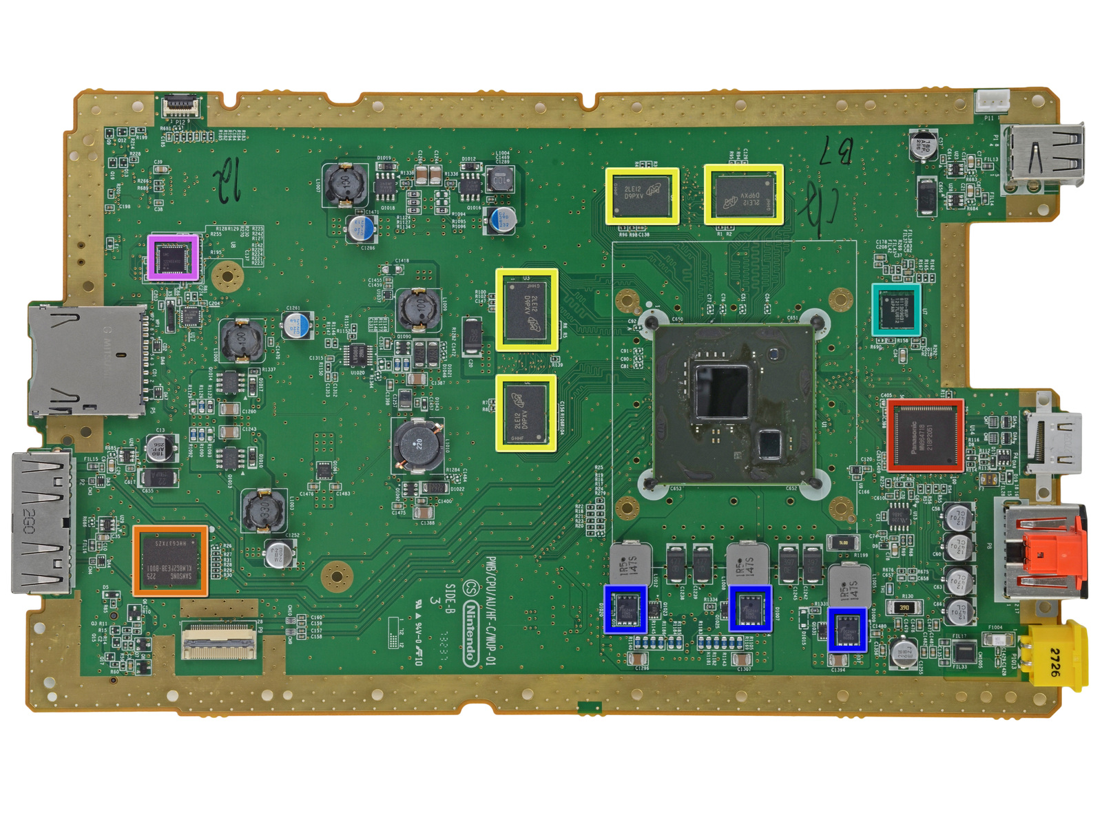
What about you? Can you look at a picture of the Wii U's motherboard or GPU and derive conclusions? If so, go!
Weren't we talking about floating point performance? How do you know all of their PS4 specs which weren't given by Sony are correct? It's easy to get specification right if you are given them in the first place. There isn't a device on the motherboard that tells us the theoretical performance of the Wii U. People have to figure that out. It is entirely different from counting certain features by looking at the physical component on the board. There are assumptions involved, and calculations to be made. Here is the analysis that ended with 178-350 gflops by the way. Notice how they mention that the GPU isn't just a r700. http://www.neogaf.com/forum/showthread.php?t=511628 "The die is exactly 11.88 x 12.33mm (146.48mm²). Chipworks believe that it's "fabricated in a 40 nm advanced CMOS process at TSMC". It carries Renesas die markings, but no AMD die markings (although there is an AMD marking on the MCM heat-spreader). This is unexpected, as it was widely reported that the GPU was originally based on AMD's R700 line, and Nintendo publicly referred to it as a Radeon-based GPU. As the die appears to be very highly customised (it looks very different to other R700-based GPUs), the markings (or lack thereof) may indicate that the customisations were not done by AMD, but rather by Nintendo and Renesas." "It it worth noting at this stage that a large portion of the GPU logic is still unexplained." |
hat makes their opinion more believable then the popular one?
Current Consoles: PS3, PS4, Wii U

PC Specs: i7-4770, GTX 560 Ti, 12GB 1600Mhz DDR3


