










Pemalite said:
Not exactly. |
Actually FinFET isn't related to chip area scaling at ALL. It's just a different transistor technology. The reason why we made our move to FinFETs in the first place is because planar MOFSET technology wasn't going to scale well in performance when moving down to below 20nm. When TSMC makes their first move to FinFET they will have no chip area scaling to go with it.
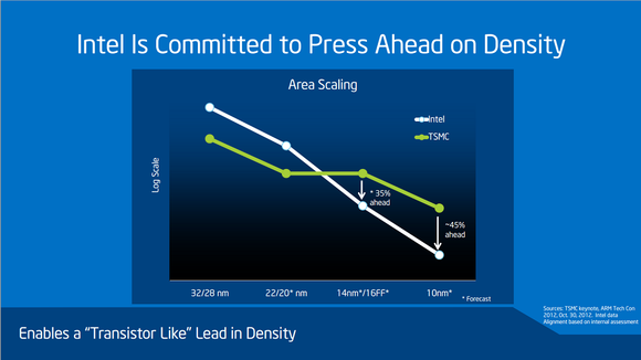
If your wondering why globalfoundries and samsung has a 15% advantage in chip area scaling when making the move to FinFET compared to TSMC's 20/16nm process node it is because samsung has applied more work to the contact pitch in order to increase density.