


Aielyn said:
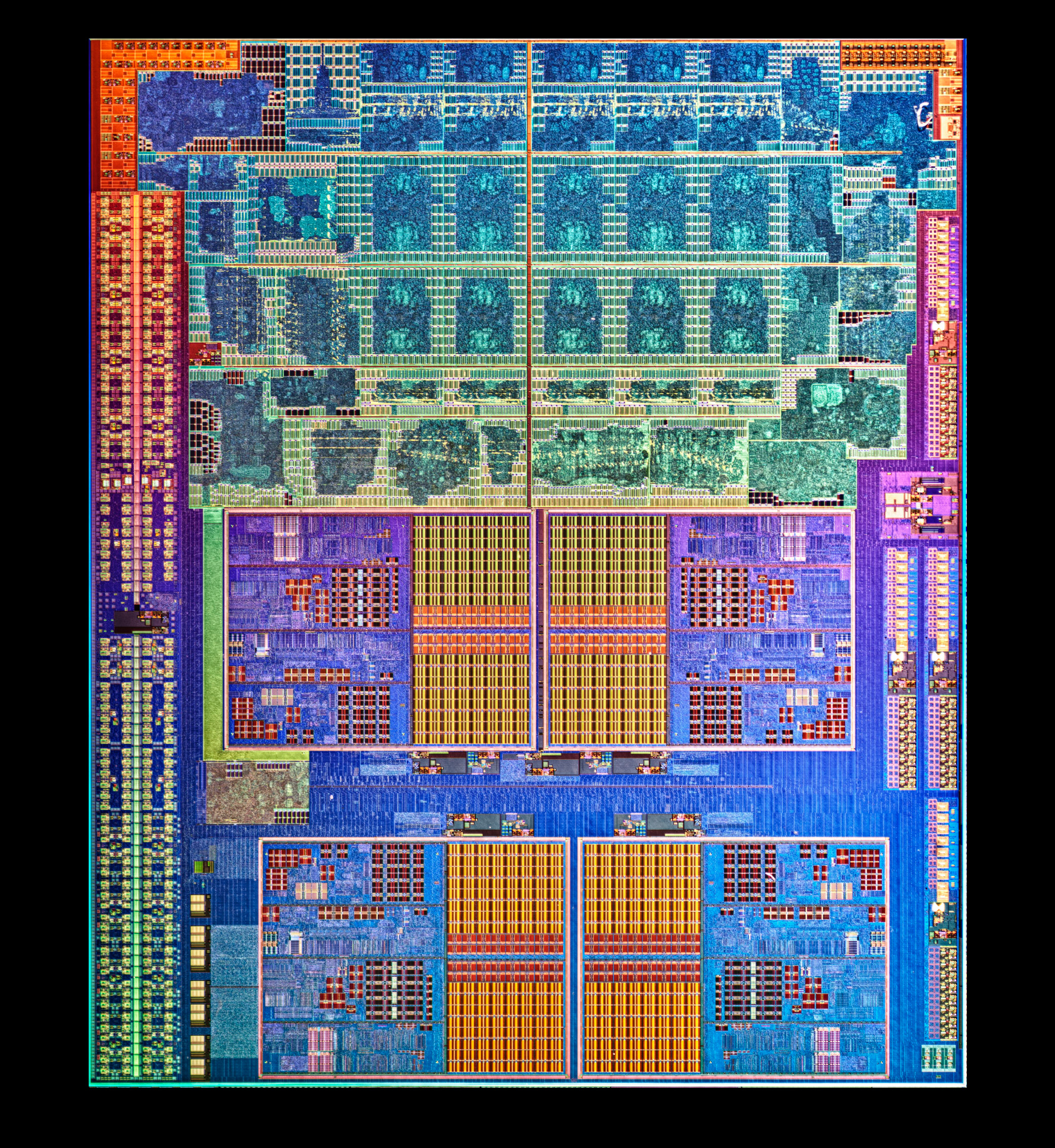
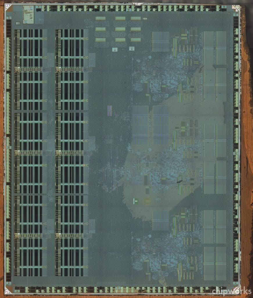
I think you've misunderstood the question. It's not "what if the GPU has HSA technology in how it works with the CPU?" It's "what if the GPU also contains more CPU circuitry, and thus is closer to being an APU?" After all, we've heard repeatedly that the GPU in the Wii U is meant to basically be a GPGPU, and my understanding is that AMD's HSA technology is meant to be their equivalent of a GPGPU, just in the form of an APU. It might explain why we've got so much conflicting information. I even see what I think is a plausible location for it - feature D on the annotated die image. Mind you, I'm no expert - I'm just looking for similarities between Llano and the Wii U CPU and GPU dies. There are some structures in D that resemble structures in the CPU part of Llano (the bottom part of this image), and aren't all that dissimilar to the right side of the CPU (this image), where the actual CPU components are (the left side has the memory). And if you compare the size of D with the size of the CPU cores (you can recognise them based on the fact that there are three cores, and the middle one has four times the cache), it actually comes out damn close. It doesn't necessarily have to have any physical CPU core - just some of the logic, etc. |
I guess my understanding of the HSA technology was wrong, then. I thought it was only applicable to APU solutions and not on separate CPU+GPU solutions. Based on what i understood, you're talking about the GPU containing some CPU logic and thus being somewhat an APU, so Wii U's MCM would actually contain a CPU and an APU, is that right? That's actually a quite interesting theory and, in theory, it would be possible, altough i don't see why Nintendo would choose to use a separate CPU and an APU instead of just using one big die with both the GPU and a complete CPU, not just some logic, in a more common APU setting. It would also explain Iwata talking about how important the GPGPU functionality of the console is, even if the GPU had only 160SPs, for example, the embedded CPU logic would give the GPGPU funcionality quite a boost. However, I don't think AMD would allow to put IBM's CPU design on their APU chip, and if AMD did that CPU logic inside the GPU, then there would be a lot of problems utilizing it thanks to the difference in x86 and PowerPC achitecture. I mean, i'm no expert either, so what i'm talking here might be worth nothing, but what you said could be possible, after all, there's still 30% unknown in that GPU and this unknown part is close to where you pointed.
