The final specs and official slides of the GTX 1080 have been leaked:
NVIDIA GeForce GTX 1080 Final Specifications and Launch Presentation
http://videocardz.com/59962/nvidia-geforce-gtx-1080-final-specifications-and-launch-presentation
NVIDIA GTX 1080 is the first graphics card from GeForce 1000, or as NVIDIA calls it 10 Series, based on 16nm FinFET architecture called Pascal. New card is clocked at 1607 MHz with boost clock up to 1733 MHz, however actual clock will vary depending on application.
NVIDIA GTX 1080 is equipped with one 8-pin power connectors and TDP is rated at 180W, and from what I heard, actual power consumption should not exceed this value in gaming.
| NVIDIA GeForce GTX 1080 Specifications |
| May 15th 2016 | GeForce GTX 1080 | GeForce GTX 980 Ti | GeForce GTX 980 |
| Fabrication Node |
16nm FinFET |
28nm |
28nm |
| Architecture |
Pascal |
Maxwell |
Maxwell |
| Die Size |
314 mm2 |
601 mm2 |
398 mm2 |
| GPU |
GP104-400 |
GM200-310 |
GM204-400 |
| Transistors |
7.2 b |
8.0 b |
5.2 b |
| Transistors per mm2 |
~22.9 m |
~13.3 m |
~13.1 m |
| Streaming Multiprocessors |
20 |
22 |
16 |
| CUDA Cores |
2560 |
2816 |
2048 |
| TMUs |
160 |
176 |
128 |
| ROPs |
64 |
96 |
64 |
| TFLOPs |
8.2 TFLOPs |
5.6 TFLOPs |
4.6 TFLOPS |
| Memory Type |
8GB GDDR5X |
6GB GDDR5 |
4GB GDDR5 |
| Base Clock |
1607 MHz |
1000 MHz |
1127 MHz |
| Boost Clock |
1733 MHz |
1076 MHz |
1216 MHz |
| Memory Clock |
1250 MHz |
1750 MHz |
1750 MHz |
| Effective Memory Clock |
10000 MHz |
7000 MHz |
7000 MHz |
| Memory Bus |
256-bit |
384-bit |
256-bit |
| Memory Bandwidth |
320 GB/s |
337 GB/s |
224 GB/s |
| TDP |
180W |
250W |
165W |
| Power Connectors |
1x 8pin |
1x 6pin + 1x 8pin |
2x 6pin |
| MSRP |
$599
$699 FE |
$649 |
$549 |
NVIDIA GeForce GTX 1080 has 160 TMUs and 64 ROPs. This was actually confirmed earlier by GPU-Z update, but today our knowledge is based on official GPU diagram, which looks like this:
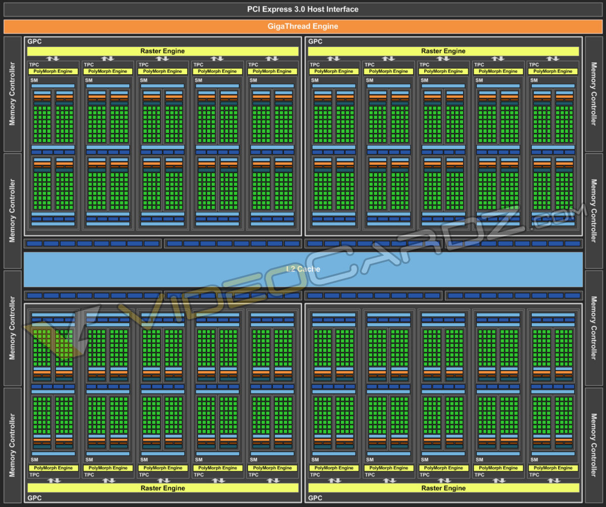
As you can see Pascal GP104 is split into four blocks (Graphics Processing Clusters), each GPC has 5 Streaming Multiprocessors and each SM has two blocks of 64 CUDA cores, so this gives us total of 2560 CUDA Cores. As a side note, GP100 only has one block of 64 CUDAs per SM.
Interestingly the number of ROPs has not changed since GTX 980, which means GTX 980 Ti still has 32 ROPs more, and therefore GTX 1080 has 64 ROPs.
The die area of GP104 GPU is 314 mm2, which is right in-between GM204 and GM206. Despite smaller GPU we have 2 billion transistors more than GM204. Also the density of transistors increased by 10 million per mm2 to almost 23 million.

Check out the link for more details and slides.
Please excuse my bad English.
Currently gaming on a PC with an i5-4670k@stock (for now), 16Gb RAM 1600 MHz and a GTX 1070
Steam / Live / NNID : jonxiquet Add me if you want, but I'm a single player gamer.