By using this site, you agree to our Privacy Policy and our Terms of Use. Close

Forums - PC Discussion - PS4-architecture to be used in future APUs - AMD shows

Remember Cerny's talk last week about some crucial changes in PS4-architecture they did with AMD to differentiate it to standard-PCs? This differentiation will be no more, according to several news-sites: (This one taken from http://hothardware.com/News/AMD-Announces-hUMA-Heterogeneous-Uniform-Memory-Access-For-Future-APUs/ )

"AMD Announces hUMA, Heterogeneous Uniform Memory Access For Future APUs

Tuesday, April 30, 2013 - by Marco Chiappetta


The dawn of GPU computing came about in large part due to the immense gap in compute performance between traditional CPUs and programmable GPUs. Whereas CPUs excel with serial workloads, modern GPUs perform best with highly parallel operations. If you look at the slide below, it shows an array of Intel processors and AMD (and ATI) GPUs dating back to 2002, along with each part’s compute performance, measured in GFLOPS (or Gigaflops—billions of floating point operations per second). It gives a number of examples that show the clear disparities in compute performance we’re talking about.


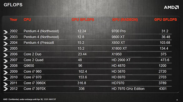
As you can see, even today’s fastest desktop processor, the 6-core / 12-thread Intel Core i7-3970X, offers much lower floating point compute performance than the roughly seven year old Radeon HD X1950. And in comparison to a contemporary GPU like the Radeon HD 7970 GHz Edition, which is outfitted with 2,048 individual stream processors, there is simply no contest. With a highly parallel, floating point intensive workload, a GPU like the Radeon HD 7970 GHz Edition can offer almost 13x the performance of the Core i7-3970X. 


 Although GPUs can theoretically offer significant performance, and sometimes power efficiency, benefits to software developers, leveraging those capabilities can often be difficult because today’s CPUs and GPUs require their own memory spaces and programming models. We’re going to simplify this explanation a bit, but what that means is that if a developer would like to leverage both CPU and GPU compute resources with a particular piece of software, the CPU must first operate within its own memory space, then the CPU must copy the requisite data to the GPU’s memory space across a relatively slow IO bus, where the GPU then completes any necessary computation, and finally the CPU must copy the results back to its memory space. Needless to say, there’s lots of inefficiency and latency introduced in a non-unified memory architecture like this, which in turn leaves plenty of performance on the table. AMD wants to change that. 


 Today AMD is announcing hUMA or Heterogeneous Unified Memory Access. AMD been talking about some of the features of hUMA for a while, but is now ready to disclose more specifics and they've got a product that employs the technology already waiting in the wings. 


 To better understand hUMA, we should first talk a bit about the UMA (Uniform Memory Access) and NUMA (Non-Unified Memory Access) architectures prevalent today. The original meaning of UMA is Uniform Memory Access and it refers to how the processing cores in a system view and access memory. In a UMA-capable architecture, all processing cores share a single memory address space. There is a single memory heap and all CPU cores can access any address. 


 The introduction of GPU computing, however, created systems with Non-Uniform Memory Access, or NUMA. NUMA requires data to be managed across multiple heaps with different address spaces for the CPUs and GPUs, which adds programming complexity due to frequent copies, synchronization, and address translation, as we mentioned above. There are also power and performance inefficiencies inherent to NUMA architectures because data is often duplicated and shuttled on and off chips over external busses.


In the slide shown here, there are a couple of basic block diagrams that illustrate UMA, NUMA, and hUMA. The top row in the slide shows four CPUs accessing a single pool of memory in a bi-directional, cohesive manner in a UMA configuration. The next row represents a NUMA architecture, with CPUs and GPUs accessing separate memory blocks. In the NUMA configuration, there are discrete pools or heaps of memory for the CPUs and GPUs and the they each operate only within their own pools of memory. Things come full circle with hUMA though, with both the CPUs and GPUs accessing the entire memory space with bi-directional coherency.


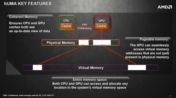
The main features of hUMA are:

Bi-Directional Coherent Memory - Any updates made by one processing element will be seen by all other processing elements, GPU or CPU


Pageable Memory - GPU can take page faults, and is no longer restricted to page locked memory


Entire Memory Space - CPU and GPU processes can dynamically allocate memory from the entire memory space 


This is how current NUMA architectures operate...


With hUMA, the CPU and GPU and share data in a uniform memory space.


AMD claims that programming for hUMA-enabled platforms should ease software development and potentially lower development costs as well. The technology is supported by mainstream programming languages like Python, C++, and Java, and should allow developers to more simply code for a particular compute resource with no need for special APIs. AMD also points out that there’s a level of power efficiency introduced with hUMA because parallel code that used to run on CPU can now be run on the GPU, and vice versa. 


 If you’ve wondering when hUMA-enabled products will hit the market, we’re told Kaveri will be the first APU to support the technology. Kaveri is the codename of AMD’s first APU built around the company’s Steamroller cores, which should offer significant performance improvements over current Piledriver-based products. Expect Kaveri to launch some time in the second half of 2013."


Around the Network

Seems like the PS4 will no longer have the upper hand against PC.


Nintendo is selling their IPs to Microsoft and this is true because:

http://gamrconnect.vgchartz.com/thread.php?id=221391&page=1

AbbathTheGrim said:
Seems like the PS4 will no longer have the upper hand against PC.


Yes, even in an architectural way, there is no advantage anymore when AMD releases this. I was wondering last week if this was all due to Cerny visiting devs and told AMD to develop for Sony or if AMD had already plans to do this and Sony just jumped on the train. 

We will see if NextBox also uses this, then it's definitely invented by AMD and not Sony. The only difference remaining is GDDR5.


this is why PS4 will be cheaper!


walsufnir said:
AbbathTheGrim said:
Seems like the PS4 will no longer have the upper hand against PC.


Yes, even in an architectural way, there is no advantage anymore when AMD releases this. I was wondering last week if this was all due to Cerny visiting devs and told AMD to develop for Sony or if AMD had already plans to do this and Sony just jumped on the train. 

We will see if NextBox also uses this, then it's definitely invented by AMD and not Sony. The only difference remaining is GDDR5.

http://www.theinquirer.net/inquirer/news/2250802/amd-to-sell-a-cut-down-version-of-sonys-playstation-4-apu  


AMD to sell a cut down version of Sony's Playstation 4 APU

Will show how much work Sony has done


CHIP DESIGNER AMD will offer a cut down version of the APU chip that will be in Sony's Playstation 4 later this year.

...

However John Taylor, head of marketing for AMD's Global Business Units, said that a version of the same chip without Sony's technology will be available for consumers later this year.

Taylor told The INQUIRER that the AMD branded APU chip will not have the same number of cores or the same computing capability as Sony's part.

...

Taylor said that this is all part of AMD's "flexible system on chip strategy", but what the upcoming A-series parts will show is just how much work Sony put into the chip that is found in the Playstation 4.

Sounds like Sony had quite a hand in the PS4's APU.


Around the Network
Sal.Paradise said:
walsufnir said:
AbbathTheGrim said:
Seems like the PS4 will no longer have the upper hand against PC.


Yes, even in an architectural way, there is no advantage anymore when AMD releases this. I was wondering last week if this was all due to Cerny visiting devs and told AMD to develop for Sony or if AMD had already plans to do this and Sony just jumped on the train. 

We will see if NextBox also uses this, then it's definitely invented by AMD and not Sony. The only difference remaining is GDDR5.

http://www.theinquirer.net/inquirer/news/2250802/amd-to-sell-a-cut-down-version-of-sonys-playstation-4-apu  


AMD to sell a cut down version of Sony's Playstation 4 APU

Will show how much work Sony has done


CHIP DESIGNER AMD will offer a cut down version of the APU chip that will be in Sony's Playstation 4 later this year.

...

However John Taylor, head of marketing for AMD's Global Business Units, said that a version of the same chip without Sony's technology will be available for consumers later this year.

Taylor told The INQUIRER that the AMD branded APU chip will not have the same number of cores or the same computing capability as Sony's part.

...

Taylor said that this is all part of AMD's "flexible system on chip strategy", but what the upcoming A-series parts will show is just how much work Sony put into the chip that is found in the Playstation 4.

Sounds like Sony had quite a hand in the PS4's APU.


"He said, "Everything that Sony has shared in that single chip is AMD [intellectual property], but we have not built an APU quite like that for anyone else in the market." 


As I read the article it's the number of cores that is Sony's "tech".


walsufnir said:
Sal.Paradise said:
walsufnir said:
AbbathTheGrim said:
Seems like the PS4 will no longer have the upper hand against PC.


Yes, even in an architectural way, there is no advantage anymore when AMD releases this. I was wondering last week if this was all due to Cerny visiting devs and told AMD to develop for Sony or if AMD had already plans to do this and Sony just jumped on the train. 

We will see if NextBox also uses this, then it's definitely invented by AMD and not Sony. The only difference remaining is GDDR5.

http://www.theinquirer.net/inquirer/news/2250802/amd-to-sell-a-cut-down-version-of-sonys-playstation-4-apu  


AMD to sell a cut down version of Sony's Playstation 4 APU

Will show how much work Sony has done


CHIP DESIGNER AMD will offer a cut down version of the APU chip that will be in Sony's Playstation 4 later this year.

...

However John Taylor, head of marketing for AMD's Global Business Units, said that a version of the same chip without Sony's technology will be available for consumers later this year.

Taylor told The INQUIRER that the AMD branded APU chip will not have the same number of cores or the same computing capability as Sony's part.

...

Taylor said that this is all part of AMD's "flexible system on chip strategy", but what the upcoming A-series parts will show is just how much work Sony put into the chip that is found in the Playstation 4.

Sounds like Sony had quite a hand in the PS4's APU.


"He said, "Everything that Sony has shared in that single chip is AMD [intellectual property], but we have not built an APU quite like that for anyone else in the market." 


As I read the article it's the number of cores that is Sony's "tech".


The 'number of cores' and the 'computing capabilities.' This probably has a lot to do with the customizations we've heard about from Cerny so far, especially how much he talks about compute:

The three "major modifications" Sony did to the architecture to support this vision are as follows, in Cerny's words:

  • "First, we added another bus to the GPU that allows it to read directly from system memory or write directly to system memory, bypassing its own L1 and L2 caches. As a result, if the data that's being passed back and forth between CPU and GPU is small, you don't have issues with synchronization between them anymore. And by small, I just mean small in next-gen terms. We can pass almost 20 gigabytes a second down that bus. That's not very small in today’s terms -- it’s larger than the PCIe on most PCs!
  • "Next, to support the case where you want to use the GPU L2 cache simultaneously for both graphics processing and asynchronous compute, we have added a bit in the tags of the cache lines, we call it the 'volatile' bit. You can then selectively mark all accesses by compute as 'volatile,' and when it's time for compute to read from system memory, it can invalidate, selectively, the lines it uses in the L2. When it comes time to write back the results, it can write back selectively the lines that it uses. This innovation allows compute to use the GPU L2 cache and perform the required operations without significantly impacting the graphics operations going on at the same time -- in other words, it radically reduces the overhead of running compute and graphics together on the GPU."
  • Thirdly, said Cerny, "The original AMD GCN architecture allowed for one source of graphics commands, and two sources of compute commands. For PS4, we’ve worked with AMD to increase the limit to 64 sources of compute commands -- the idea is if you have some asynchronous compute you want to perform, you put commands in one of these 64 queues, and then there are multiple levels of arbitration in the hardware to determine what runs, how it runs, and when it runs, alongside the graphics that's in the system."

"The reason so many sources of compute work are needed is that it isn’t just game systems that will be using compute -- middleware will have a need for compute as well. And the middleware requests for work on the GPU will need to be properly blended with game requests, and then finally properly prioritized relative to the graphics on a moment-by-moment basis."

This concept grew out of the software Sony created, called SPURS, to help programmers juggle tasks on the CELL's SPUs -- but on the PS4, it's being accomplished in hardware.

The team, to put it mildly, had to think ahead. "The time frame when we were designing these features was 2009, 2010. And the timeframe in which people will use these features fully is 2015? 2017?" said Cerny.

"Our overall approach was to put in a very large number of controls about how to mix compute and graphics, and let the development community figure out which ones they want to use when they get around to the point where they're doing a lot of asynchronous compute."

Cerny expects developers to run middleware -- such as physics, for example -- on the GPU. Using the system he describes above, you can run at peak efficiency, he said.

"If you look at the portion of the GPU available to compute throughout the frame, it varies dramatically from instant to instant. For example, something like opaque shadow map rendering doesn't even use a pixel shader, it’s entirely done by vertex shaders and the rasterization hardware -- so graphics aren't using most of the 1.8 teraflops of ALU available in the CUs. Times like that during the game frame are an opportunity to say, 'Okay, all that compute you wanted to do, turn it up to 11 now.'"

Sounds great -- but how do you handle doing that? "There are some very simple controls where on the graphics side, from the graphics command buffer, you can crank up or down the compute," Cerny said. "The question becomes, looking at each phase of rendering and the load it places on the various GPU units, what amount and style of compute can be run efficiently during that phase?"


Sal.Paradise said:
walsufnir said:
Sal.Paradise said:
walsufnir said:
AbbathTheGrim said:
Seems like the PS4 will no longer have the upper hand against PC.


Yes, even in an architectural way, there is no advantage anymore when AMD releases this. I was wondering last week if this was all due to Cerny visiting devs and told AMD to develop for Sony or if AMD had already plans to do this and Sony just jumped on the train. 

We will see if NextBox also uses this, then it's definitely invented by AMD and not Sony. The only difference remaining is GDDR5.

http://www.theinquirer.net/inquirer/news/2250802/amd-to-sell-a-cut-down-version-of-sonys-playstation-4-apu  


AMD to sell a cut down version of Sony's Playstation 4 APU

Will show how much work Sony has done


CHIP DESIGNER AMD will offer a cut down version of the APU chip that will be in Sony's Playstation 4 later this year.

...

However John Taylor, head of marketing for AMD's Global Business Units, said that a version of the same chip without Sony's technology will be available for consumers later this year.

Taylor told The INQUIRER that the AMD branded APU chip will not have the same number of cores or the same computing capability as Sony's part.

...

Taylor said that this is all part of AMD's "flexible system on chip strategy", but what the upcoming A-series parts will show is just how much work Sony put into the chip that is found in the Playstation 4.

Sounds like Sony had quite a hand in the PS4's APU.


"He said, "Everything that Sony has shared in that single chip is AMD [intellectual property], but we have not built an APU quite like that for anyone else in the market." 


As I read the article it's the number of cores that is Sony's "tech".


The 'number of cores' and the 'computing capabilities.' This probably has a lot to do with the customizations we've heard about from Cerny so far, especially how much he talks about compute:


The three "major modifications" Sony did to the architecture to support this vision are as follows, in Cerny's words:

  • "First, we added another bus to the GPU that allows it to read directly from system memory or write directly to system memory, bypassing its own L1 and L2 caches. As a result, if the data that's being passed back and forth between CPU and GPU is small, you don't have issues with synchronization between them anymore. And by small, I just mean small in next-gen terms. We can pass almost 20 gigabytes a second down that bus. That's not very small in today’s terms -- it’s larger than the PCIe on most PCs!
  • "Next, to support the case where you want to use the GPU L2 cache simultaneously for both graphics processing and asynchronous compute, we have added a bit in the tags of the cache lines, we call it the 'volatile' bit. You can then selectively mark all accesses by compute as 'volatile,' and when it's time for compute to read from system memory, it can invalidate, selectively, the lines it uses in the L2. When it comes time to write back the results, it can write back selectively the lines that it uses. This innovation allows compute to use the GPU L2 cache and perform the required operations without significantly impacting the graphics operations going on at the same time -- in other words, it radically reduces the overhead of running compute and graphics together on the GPU."
  • Thirdly, said Cerny, "The original AMD GCN architecture allowed for one source of graphics commands, and two sources of compute commands. For PS4, we’ve worked with AMD to increase the limit to 64 sources of compute commands -- the idea is if you have some asynchronous compute you want to perform, you put commands in one of these 64 queues, and then there are multiple levels of arbitration in the hardware to determine what runs, how it runs, and when it runs, alongside the graphics that's in the system."

I know what he said but the cache-stuff seems to translate directly to what HUMA actually is. If you look at the HUMA-design it especially means that both cpu and gpu share the memory-pool and caches. There is of course details lacking. But this is another evolution of the standard apu AMD delivers today and the changes do look a lot like what Sony also said the changes were.

This doesn't mean that there is nothing more Sony added to the tech but your source only says "more cores", no matter what Cerny said also.


walsufnir said:
Sal.Paradise said:
walsufnir said:
Sal.Paradise said:
walsufnir said:
AbbathTheGrim said:
Seems like the PS4 will no longer have the upper hand against PC.


Yes, even in an architectural way, there is no advantage anymore when AMD releases this. I was wondering last week if this was all due to Cerny visiting devs and told AMD to develop for Sony or if AMD had already plans to do this and Sony just jumped on the train. 

We will see if NextBox also uses this, then it's definitely invented by AMD and not Sony. The only difference remaining is GDDR5.

http://www.theinquirer.net/inquirer/news/2250802/amd-to-sell-a-cut-down-version-of-sonys-playstation-4-apu  


AMD to sell a cut down version of Sony's Playstation 4 APU

Will show how much work Sony has done


CHIP DESIGNER AMD will offer a cut down version of the APU chip that will be in Sony's Playstation 4 later this year.

...

However John Taylor, head of marketing for AMD's Global Business Units, said that a version of the same chip without Sony's technology will be available for consumers later this year.

Taylor told The INQUIRER that the AMD branded APU chip will not have the same number of cores or the same computing capability as Sony's part.

...

Taylor said that this is all part of AMD's "flexible system on chip strategy", but what the upcoming A-series parts will show is just how much work Sony put into the chip that is found in the Playstation 4.

Sounds like Sony had quite a hand in the PS4's APU.


"He said, "Everything that Sony has shared in that single chip is AMD [intellectual property], but we have not built an APU quite like that for anyone else in the market." 


As I read the article it's the number of cores that is Sony's "tech".


The 'number of cores' and the 'computing capabilities.' This probably has a lot to do with the customizations we've heard about from Cerny so far, especially how much he talks about compute:


The three "major modifications" Sony did to the architecture to support this vision are as follows, in Cerny's words:

  • "First, we added another bus to the GPU that allows it to read directly from system memory or write directly to system memory, bypassing its own L1 and L2 caches. As a result, if the data that's being passed back and forth between CPU and GPU is small, you don't have issues with synchronization between them anymore. And by small, I just mean small in next-gen terms. We can pass almost 20 gigabytes a second down that bus. That's not very small in today’s terms -- it’s larger than the PCIe on most PCs!
  • "Next, to support the case where you want to use the GPU L2 cache simultaneously for both graphics processing and asynchronous compute, we have added a bit in the tags of the cache lines, we call it the 'volatile' bit. You can then selectively mark all accesses by compute as 'volatile,' and when it's time for compute to read from system memory, it can invalidate, selectively, the lines it uses in the L2. When it comes time to write back the results, it can write back selectively the lines that it uses. This innovation allows compute to use the GPU L2 cache and perform the required operations without significantly impacting the graphics operations going on at the same time -- in other words, it radically reduces the overhead of running compute and graphics together on the GPU."
  • Thirdly, said Cerny, "The original AMD GCN architecture allowed for one source of graphics commands, and two sources of compute commands. For PS4, we’ve worked with AMD to increase the limit to 64 sources of compute commands -- the idea is if you have some asynchronous compute you want to perform, you put commands in one of these 64 queues, and then there are multiple levels of arbitration in the hardware to determine what runs, how it runs, and when it runs, alongside the graphics that's in the system."

I know what he said but the cache-stuff seems to translate directly to what HUMA actually is. If you look at the HUMA-design it especially means that both cpu and gpu share the memory-pool and caches. There is of course details lacking. But this is another evolution of the standard apu AMD delivers today and the changes do look a lot like what Sony also said the changes were.

This doesn't mean that there is nothing more Sony added to the tech but your source only says "more cores", no matter what Cerny said also. 


My source , AMD themselves, says will not have the same number of cores or the same computing capability as Sony's part. What specific parts of those will remain unique to the PS4's APU, we should find out when the consumer PC version releases.

Still, what my source shows is "just how much work Sony put into the chip that is found in the Playstation 4."  Which is the reason I posted here in the first place, after you implying Sony may not have had a hand in any of the PS4's APU, or that GDDR5 will be the only difference, which my source shows is not true. 


Sal.Paradise said:
walsufnir said:
Sal.Paradise said:
walsufnir said:
Sal.Paradise said:
walsufnir said:
AbbathTheGrim said:
Seems like the PS4 will no longer have the upper hand against PC.


Yes, even in an architectural way, there is no advantage anymore when AMD releases this. I was wondering last week if this was all due to Cerny visiting devs and told AMD to develop for Sony or if AMD had already plans to do this and Sony just jumped on the train. 

We will see if NextBox also uses this, then it's definitely invented by AMD and not Sony. The only difference remaining is GDDR5.

http://www.theinquirer.net/inquirer/news/2250802/amd-to-sell-a-cut-down-version-of-sonys-playstation-4-apu  


AMD to sell a cut down version of Sony's Playstation 4 APU

Will show how much work Sony has done


CHIP DESIGNER AMD will offer a cut down version of the APU chip that will be in Sony's Playstation 4 later this year.

...

However John Taylor, head of marketing for AMD's Global Business Units, said that a version of the same chip without Sony's technology will be available for consumers later this year.

Taylor told The INQUIRER that the AMD branded APU chip will not have the same number of cores or the same computing capability as Sony's part.

...

Taylor said that this is all part of AMD's "flexible system on chip strategy", but what the upcoming A-series parts will show is just how much work Sony put into the chip that is found in the Playstation 4.

Sounds like Sony had quite a hand in the PS4's APU.


"He said, "Everything that Sony has shared in that single chip is AMD [intellectual property], but we have not built an APU quite like that for anyone else in the market." 


As I read the article it's the number of cores that is Sony's "tech".


The 'number of cores' and the 'computing capabilities.' This probably has a lot to do with the customizations we've heard about from Cerny so far, especially how much he talks about compute:


The three "major modifications" Sony did to the architecture to support this vision are as follows, in Cerny's words:

  • "First, we added another bus to the GPU that allows it to read directly from system memory or write directly to system memory, bypassing its own L1 and L2 caches. As a result, if the data that's being passed back and forth between CPU and GPU is small, you don't have issues with synchronization between them anymore. And by small, I just mean small in next-gen terms. We can pass almost 20 gigabytes a second down that bus. That's not very small in today’s terms -- it’s larger than the PCIe on most PCs!
  • "Next, to support the case where you want to use the GPU L2 cache simultaneously for both graphics processing and asynchronous compute, we have added a bit in the tags of the cache lines, we call it the 'volatile' bit. You can then selectively mark all accesses by compute as 'volatile,' and when it's time for compute to read from system memory, it can invalidate, selectively, the lines it uses in the L2. When it comes time to write back the results, it can write back selectively the lines that it uses. This innovation allows compute to use the GPU L2 cache and perform the required operations without significantly impacting the graphics operations going on at the same time -- in other words, it radically reduces the overhead of running compute and graphics together on the GPU."
  • Thirdly, said Cerny, "The original AMD GCN architecture allowed for one source of graphics commands, and two sources of compute commands. For PS4, we’ve worked with AMD to increase the limit to 64 sources of compute commands -- the idea is if you have some asynchronous compute you want to perform, you put commands in one of these 64 queues, and then there are multiple levels of arbitration in the hardware to determine what runs, how it runs, and when it runs, alongside the graphics that's in the system."

I know what he said but the cache-stuff seems to translate directly to what HUMA actually is. If you look at the HUMA-design it especially means that both cpu and gpu share the memory-pool and caches. There is of course details lacking. But this is another evolution of the standard apu AMD delivers today and the changes do look a lot like what Sony also said the changes were.

This doesn't mean that there is nothing more Sony added to the tech but your source only says "more cores", no matter what Cerny said also. 


My source , AMD themselves, says will not have the same number of cores or the same computing capability as Sony's part. What specific parts of those will remain unique to the PS4's APU, we should find out when the consumer PC version releases.

Still, what my source shows is "just how much work Sony put into the chip that is found in the Playstation 4."  Which is the reason I posted here in the first place, after you implying Sony may not have had a hand in any of the PS4's APU, or that GDDR5 will be the only difference, which my source shows is not true. 


Yes, in this point you seem to be right and I am wrong but still we don't know what exactly is what Sony contributed.