| Pemalite said: "Electronic circuits" still have significant room to exponentially grow and become more complex... And thus will enable new rendering paradigms. |
Everyone and their mother in the industry knows there are at best a handful of full nodes left and then they are moving on to vertical circuit stacking. This isn't exactly a secret or an opinion:
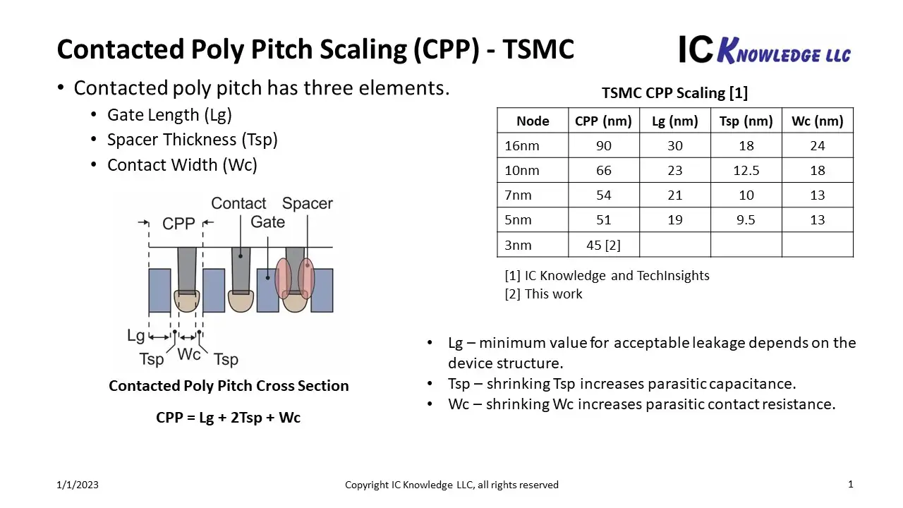
Regardless of TSMC's shenanigans, ITRS's nomenclature has never referred to the physical size of transistors. Historically it was half of the gate pitch which was a close approximation for the smallest feature size of a MOSFET.
That hasn't been the case for a long time, however, as logic scales better than the rest of the circuit:

TSMC's 3 nm transistors have logic gates of ~ 15 nm and within them transistors with silicon fins as small as 7 nm wide, which is pretty close to electron mobility collapse from quantum tunneling.
Even using theoretical 2D materials and 1 nm transistors as wide as a single molecule isn't going to make matters much better (just ~ 5 times denser than TSMC's N5).
Everyone is trying to find smarter solutions for computing problems or trying to find quantum algorithms that actually work (hint: they won't since it's very very very likely that P =/= NP) because they know brute forcing with MOSFETs isn't going to cut the mustard for much longer.
Last edited by haxxiy - on 04 August 2024


