


| JEMC said:
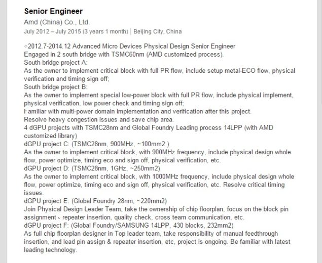
AMD 14nm FinFET POLARIS GPU SIZE LEAKS OUT – 232mm² LARGE DIE http://wccftech.com/amd-polaris-gpu-die-size-232-mm-2/ Details of AMD’s upcoming 14nm GPU have finally started leaking out. Some good detective work by the user AnarchX over at Beyond3D 3DCenter forums has revealed what appears to be the LinkedIn profile of a senior engineer at AMD. Interestingly, the engineer lists multiple projects, one of which is the Polaris die. The size of the chip will be 232mm² and (assuming the information is accurate) will constitute one tier of the Polaris architecture.
"According to the information we have about the 14nm LPP process, and based on transistor density increase, a 232mm² GPU would be roughly equivalent to a 464mm² 28nm processor – at the same TDP levels. Since we already know that AMD is going to be focusing not just on performance but power efficiency as well – this number could be be much higher, in fact we will discuss the number AMD is using below. We can however safely say that this die is more than capable of meeting the ‘minimum VR spec that AMD promises."
>>As a reference, AMD's 290/390 chips are 438 mm2, so if that assumption is true and we add the performance increases from the new architecture and other improvements, get we a chip that will bring a nice improvement in performance and power consumption while also leaving room for bigger chips down the road (either for the Fury brand or a 5x0 series) |
I would like to add that Polaris is not using TSMC's 20/16nm transistors ...
AMD is using Samsung/GlobalFoundries 14nm LPP process node with a known die area scaling advantage of upto 15% smaller die which irons out to 17% more transistors to play with in the same die sapce ...
Without accounting for other factors that don't contribute to performance such as the display engine or video codecs and etc a 232mm^2 14nm part can match a 546mm^2 28nm part in performance and get in range with 600mm^2 GPUs ...
 Essay Pro