| ethomaz said: Orbis final specs... inline with what I expected and powerful enough. GPU:
|
100% fake.
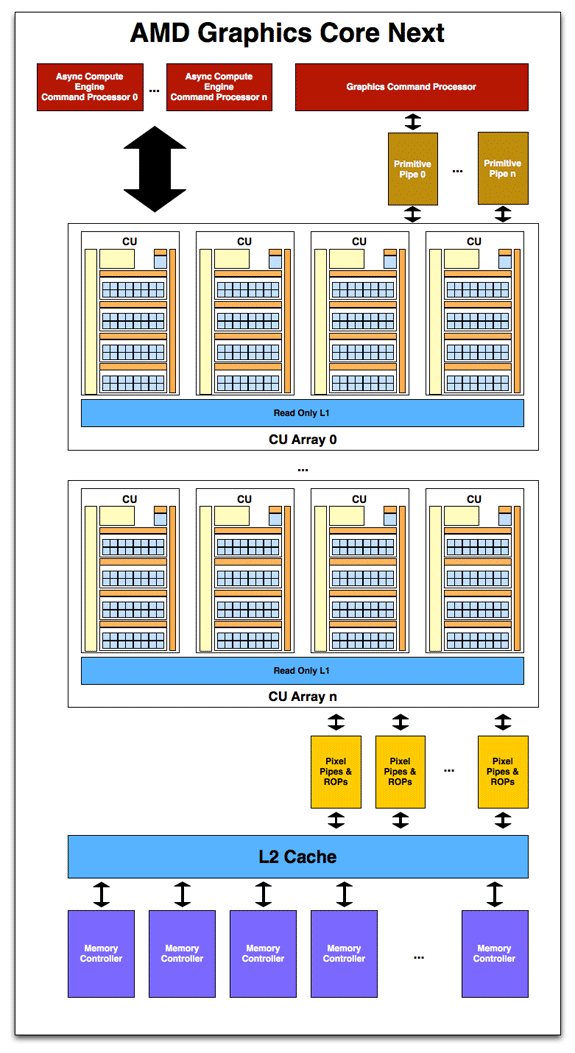
By definition of the building blocks around Graphics Core Next architecture, 1 CU is coupled with 4 TMUs (ratio of 1:4). For 18 CUs, you must have 72 Texture Units. Also, the specs for TMUs and ROPs are too weak for even the worst GPU in R1000 series. Even HD7750 has 16 ROPs and 32 TMUs. Also, the whole point beihind Graphics Core Next architecture revolves around the Compute Units being designed to perform compute work and graphics well. Why in the world would a GPU have 14+4 setup with 4 CUs allocated for compute? That's illogical because by definition of how GCN works, each CU was made for Compute work and for graphics from the ground-up. In other words, any CU can do GPGPU and you do not need to "allocate" separate CUs for GPGPU.
2 Asynchronous Compute Command Engines feed the Compute Units inside GCN to perform Compute work. Every CU is exactly the same.

...You don't need to do some weird split of 14+4 CU for compute = 18. Why is that?
"AMD’s new Asynchronous Compute Engines serve as the command processors for compute operations on GCN. The principal purpose of ACEs will be to accept work and to dispatch it off to the CUs for processing. As GCN is designed to concurrently work on several tasks, there can be multiple ACEs on a GPU, with the ACEs deciding on resource allocation, context switching, and task priority. One effect of having the ACEs is that GCN has a limited ability to execute tasks out of order. As we mentioned previously GCN is an in-order architecture, and the instruction stream on a wavefront cannot be reodered. However the ACEs can prioritize and reprioritize tasks, allowing tasks to be completed in a different order than they’re received. This allows GCN to free up the resources those tasks were using as early as possible rather than having the task consuming resources for an extended period of time in a nearly-finished state."
http://www.anandtech.com/show/4455/amds-graphics-core-next-preview-amd-architects-for-compute/5
Sounds like the person is making up specs as they go....or doesn't actually understand what they mean!! The whole point of moving from VLIW-4/5 to GCN is that each CU was made from the ground-up to perform compute work. This idea of splitting the CUs into a 14+4 group is ludicrious because the ACEs do this automatically.
Also, the rumor later states: "4 additional CUs (410 Gflops) “extra” ALU as resource for compute. Minor boost if used for rendering."
^ This statement is non-sensical. By definition of a CU, the ALUs can be used for graphics rendering or compute. If the source says the 4 extra CUs provide a minor boost for rendering, the source doesn't even understand what a CU is.
| zarx said: Sea Islands it's self is a slightly modified version of Southern Islands. Whatever custom chip that AMD have cooked up for Sony bassed on VLIW5 will likely incorperate some of the same improvements they were working on for Sea Islands. |
Southern Islands and Sea Islands are SIMD design, Graphics Core Next, not VLIW5.
http://www.anandtech.com/show/4455/amds-graphics-core-next-preview-amd-architects-for-compute/4
GCN (aka HD7000-8000 series) is the biggest architectural change for AMD graphics cards since 2007's HD2000 series.
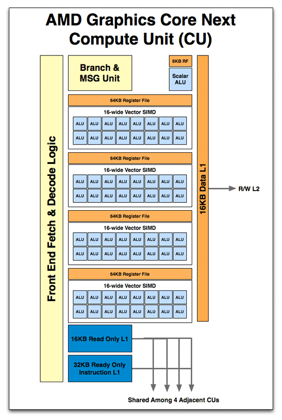
Also, people these rumors calling it "12 Shader Cores" or "18 Shader Cores" is flat out incorrect. It's 12 or 18 Compute Units. Each Compute Unit houses 64 Stream/Shader processors. So if you are talking about Shaders, it would be 768 or 1152. A Compute Unit is not a "Shader Core" as it houses 64 Shader cores inside of it.
1 Compute Unit has 64 ALUs (shader cores). To say a GPU has "12 Shader Cores" is like saying a car's horsepower is 8 cylinders....Interchanging Compute Units with Shader Cores is flat out incorrect.


