Hey viv! This might interest you (and the rest, of course). Nvidia did a Q&A session on Reddit (here's the link) and Videocardz has an article with some highlghts:
https://videocardz.com/newz/nvidia-provides-further-details-on-geforce-rtx-30-series
But here's the interesting part o what we discussed yesterday:
NVIDIA Ampere Streaming Multiprocessor
redsunstar – With regards to the expected performance of the shaders units:
- Could you elaborate a little on these doubling of CUDA cores?
- How does it affect the general architectures of the GPCs?
- How much of a challenge is it to keep all those FP32 units fed?
- What was done to ensure high occupancy?
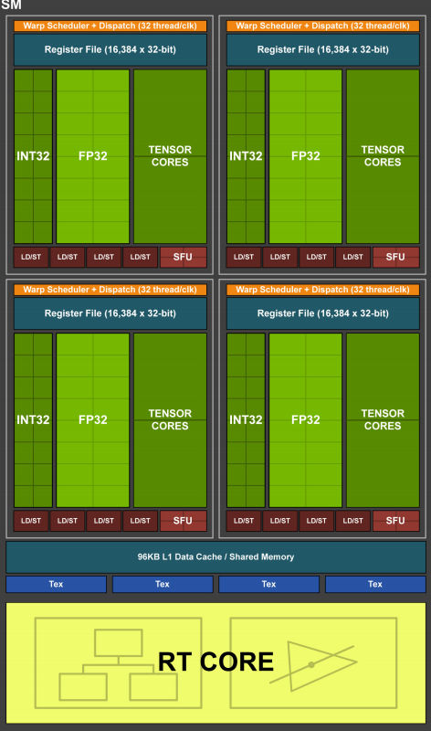
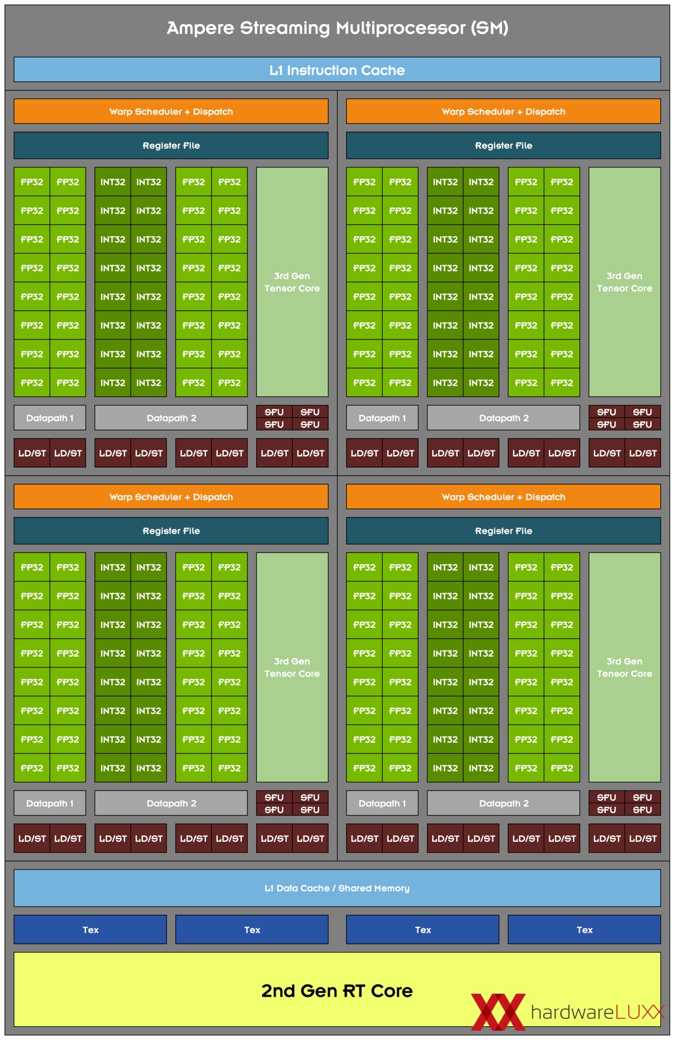
[Tony Tamasi] One of the key design goals for the Ampere 30-series SM was to achieve twice the throughput for FP32 operations compared to the Turing SM. To accomplish this goal, the Ampere SM includes new datapath designs for FP32 and INT32 operations. One datapath in each partition consists of 16 FP32 CUDA Cores capable of executing 16 FP32 operations per clock. Another datapath consists of both 16 FP32 CUDA Cores and 16 INT32 Cores. As a result of this new design, each Ampere SM partition is capable of executing either 32 FP32 operations per clock, or 16 FP32 and 16 INT32 operations per clock. All four SM partitions combined can execute 128 FP32 operations per clock, which is double the FP32 rate of the Turing SM, or 64 FP32 and 64 INT32 operations per clock.
Doubling the processing speed for FP32 improves performance for a number of common graphics and compute operations and algorithms. Modern shader workloads typically have a mixture of FP32 arithmetic instructions such as FFMA, floating point additions (FADD), or floating point multiplications (FMUL), combined with simpler instructions such as integer adds for addressing and fetching data, floating point compare, or min/max for processing results, etc. Performance gains will vary at the shader and application level depending on the mix of instructions. Ray tracing denoising shaders are good examples that might benefit greatly from doubling FP32 throughput.
Doubling math throughput required doubling the data paths supporting it, which is why the Ampere SM also doubled the shared memory and L1 cache performance for the SM. (128 bytes/clock per Ampere SM versus 64 bytes/clock in Turing). Total L1 bandwidth for GeForce RTX 3080 is 219 GB/sec versus 116 GB/sec for GeForce RTX 2080 Super.
Like prior NVIDIA GPUs, Ampere is composed of Graphics Processing Clusters (GPCs), Texture Processing Clusters (TPCs), Streaming Multiprocessors (SMs), Raster Operators (ROPS), and memory controllers.
The GPC is the dominant high-level hardware block with all of the key graphics processing units residing inside the GPC. Each GPC includes a dedicated Raster Engine, and now also includes two ROP partitions (each partition containing eight ROP units), which is a new feature for NVIDIA Ampere Architecture GA10x GPUs. More details on the NVIDIA Ampere architecture can be found in NVIDIA’s Ampere Architecture White Paper, which will be published in the coming days.
According to that, Ampere has twice the FP32 cores count than before. HardwareLUXX has done a block diagram out of that explanation:
Here's Turing with 64 cores per SM:

And here's Ampere with 128 cores per SM:
Please excuse my bad English.
Currently gaming on a PC with an i5-4670k@stock (for now), 16Gb RAM 1600 MHz and a GTX 1070
Steam / Live / NNID : jonxiquet Add me if you want, but I'm a single player gamer.


